 |
数据搜索系统,热门电子元器件搜索 |
|
|
数据搜索系统,热门电子元器件搜索 |
|
The question interval is too short.
Please try again in a few seconds.

Hello, Please ask a question about TL062IDRE4 Datasheet
# Example questions:
➢ What is the common-mode rejection ratio (cmrr) specified for the tl061c, and what test conditions are used to measure it?
➢ What is the typical input offset voltage for a tl061ac at 25°c?
➢ What is the typical supply current for each tl061c amplifier with vo = 0 and no load at 25°c?
| Part No. | TL062IDRE4 |
| Manufacturer | TI |
| Size | 975 Kbytes |
| Pages | 39 pages |
| Description | LOW-POWER JFET-INPUT OPERATIONAL AMPLIFIERS |


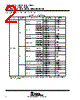


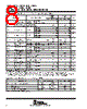



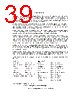

# TL06_ Series Operational Amplifiers
## Description
Low-power JFET-input operational amplifiers, designed as drop-in replacements for TL08_ series. Features high input impedance, wide bandwidth, high slew rate, and low input offset/bias currents. Available in various packages (D, P, PS, PW, JG, FK, etc.) and temperature ranges (0°C to 70°C, -40°C to 85°C, -55°C to 125°C).
## Electrical Characteristics (VCC ± = ±15V)
️· Input Offset Voltage: 3-15mV (typical)
️· Input Offset Current: 5-200pA (typical)
️· Input Bias Current: 30-400pA (typical)
️· Common-Mode Input Voltage Range: ±11 to +15V
️· Large-Signal Differential Voltage Amplification: 3-6 V/mV
️· Unity-Gain Bandwidth: 1 MHz
️· Slew Rate: 3.5 V/µs (typical)
️· CMRR: 70-86 dB
️· SVR: 70-95 dB
## Ordering Information
Available in various packages and temperature ranges with specific part numbers (e.g., TL061CP, TL062AC, TL064IN).
## Absolute Maximum Ratings
️· Supply Voltage (VCC+ / VCC−): ±18V
️· Differential Input Voltage: ±30V
️· Input Voltage: ±15V
️· Operating Junction Temperature: 150°C
️· Storage Temperature Range: -65°C to +150°C
## Key Features
️· JFET input stage
️· Low power consumption (typical 200µA per amplifier)
️· Wide bandwidth and high slew rate
️· Low input bias and offset currents
️· Common-mode input voltage range includes VCC+
️· Output short-circuit protection
️· Latch-up-free operation
# TL06_ Series Operational Amplifiers
## Description
Low-power JFET-input operational amplifiers, designed as drop-in replacements for TL08_ series. Features high input impedance, wide bandwidth, high slew rate, and low input offset/bias currents. Available in various packages (D, P, PS, PW, JG, FK, etc.) and temperature ranges (0°C to 70°C, -40°C to 85°C, -55°C to 125°C).
## Electrical Characteristics (VCC ± = ±15V)
️· Input Offset Voltage: 3-15mV (typical)
️· Input Offset Current: 5-200pA (typical)
️· Input Bias Current: 30-400pA (typical)
️· Common-Mode Input Voltage Range: ±11 to +15V
️· Large-Signal Differential Voltage Amplification: 3-6 V/mV
️· Unity-Gain Bandwidth: 1 MHz
️· Slew Rate: 3.5 V/µs (typical)
️· CMRR: 70-86 dB
️· SVR: 70-95 dB
## Ordering Information
Available in various packages and temperature ranges with specific part numbers (e.g., TL061CP, TL062AC, TL064IN).
## Absolute Maximum Ratings
️· Supply Voltage (VCC+ / VCC−): ±18V
️· Differential Input Voltage: ±30V
️· Input Voltage: ±15V
️· Operating Junction Temperature: 150°C
️· Storage Temperature Range: -65°C to +150°C
## Key Features
️· JFET input stage
️· Low power consumption (typical 200µA per amplifier)
️· Wide bandwidth and high slew rate
️· Low input bias and offset currents
️· Common-mode input voltage range includes VCC+
️· Output short-circuit protection
️· Latch-up-free operation
| Part No. | TL062IDRE4 |
| Manufacturer | TI |
| Size | 975 Kbytes |
| Pages | 39 pages |
| Description | LOW-POWER JFET-INPUT OPERATIONAL AMPLIFIERS |
| ALLDATASHEET是否为您带来帮助? [ DONATE ] |
关于 Alldatasheet | 广告服务 | 联系我们 | 隐私政策 | 数据表链接 | 链接交换 | 制造商名单 All Rights Reserved©Alldatasheet.com |
| Russian : Alldatasheetru.com | Korean : Alldatasheet.co.kr | Spanish : Alldatasheet.es | French : Alldatasheet.fr | Italian : Alldatasheetit.com Portuguese : Alldatasheetpt.com | Polish : Alldatasheet.pl | Vietnamese : Alldatasheet.vn Indian : Alldatasheet.in | Mexican : Alldatasheet.com.mx | British : Alldatasheet.co.uk | New Zealand : Alldatasheet.co.nz |
|
Family Site : ic2ic.com |
icmetro.com |
 Chinese ▼
  English
 German
 Japanese
 Russian
 Korean
 Spanish
 French
 Italian
 Portuguese
 Polish
 Vietnamese
 Indian
 Mexican
 British
 New Zealand