|
数据搜索系统,热门电子元器件搜索 |
|
|
数据搜索系统,热门电子元器件搜索 |
|
STM32L412RBU3PTR 数据表(PDF) 138 Page - STMicroelectronics |
|
|
|||||||||||||||||||||||||||||
STM32L412RBU3PTR 数据表(HTML) 138 Page - STMicroelectronics |
|
|
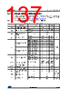
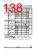
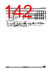
138 / 192 page  Electrical characteristics STM32L412xx 138/192 DS12469 Rev 4 The maximum value of RAIN can be found in Table 76: Maximum ADC RAIN. tLATR Trigger conversion latency Regular and injected channels without conversion abort CKMODE = 00 1.5 2 2.5 1/fADC CKMODE = 01 - - 2.0 CKMODE = 10 - - 2.25 CKMODE = 11 - - 2.125 tLATRINJ Trigger conversion latency Injected channels aborting a regular conversion CKMODE = 00 2.5 3 3.5 1/fADC CKMODE = 01 - - 3.0 CKMODE = 10 - - 3.25 CKMODE = 11 - - 3.125 ts Sampling time fADC = 80 MHz 0.03125 - 8.00625 µs - 2.5 - 640.5 1/fADC tADCVREG_STUP ADC voltage regulator start-up time -- - 20 µs tCONV Total conversion time (including sampling time) fADC = 80 MHz Resolution = 12 bits 0.1875 - 8.1625 µs Resolution = 12 bits ts + 12.5 cycles for successive approximation = 15 to 653 1/fADC IDDA(ADC) ADC consumption from the VDDA supply fs = 5 Msps - 730 830 µA fs = 1 Msps - 160 220 fs = 10 ksps - 16 50 IDDV_S(ADC) ADC consumption from the VREF+ single ended mode fs = 5 Msps - 130 160 µA fs = 1 Msps - 30 40 fs = 10 ksps - 0.6 2 IDDV_D(ADC) ADC consumption from the VREF+ differential mode fs = 5 Msps - 260 310 µA fs = 1 Msps - 60 70 fs = 10 ksps - 1.3 3 1. Guaranteed by design 2. The I/O analog switch voltage booster is enable when VDDA < 2.4 V (BOOSTEN = 1 in the SYSCFG_CFGR1 when VDDA < 2.4V). It is disable when VDDA ≥ 2.4 V. 3. VREF+ can be internally connected to VDDA and VREF- can be internally connected to VSSA, depending on the package. Refer to Section 4: Pinouts and pin description for further details. Table 75. ADC characteristics(1) (2) (continued) Symbol Parameter Conditions Min Typ Max Unit |
|
链接网址 |
| ALLDATASHEET是否为您带来帮助? [ DONATE ] |
关于 Alldatasheet | 广告服务 | 联系我们 | 隐私政策 | 数据表链接 | 链接交换 | 制造商名单 All Rights Reserved©Alldatasheet.com |
| Russian : Alldatasheetru.com | Korean : Alldatasheet.co.kr | Spanish : Alldatasheet.es | French : Alldatasheet.fr | Italian : Alldatasheetit.com Portuguese : Alldatasheetpt.com | Polish : Alldatasheet.pl | Vietnamese : Alldatasheet.vn Indian : Alldatasheet.in | Mexican : Alldatasheet.com.mx | British : Alldatasheet.co.uk | New Zealand : Alldatasheet.co.nz |
|
Family Site : ic2ic.com |
icmetro.com |
 Chinese ▼
 English
 Chinese
 German
 Japanese
 Russian
 Korean
 Spanish
 French
 Italian
 Portuguese
 Polish
 Vietnamese
 Indian
 Mexican
 British
 New Zealand