|
数据搜索系统,热门电子元器件搜索 |
|
|
数据搜索系统,热门电子元器件搜索 |
|
AM261...ZCZ 数据表(PDF) 125 Page - Texas Instruments |
|
|
|||||||||||||||||||||||||||||
AM261...ZCZ 数据表(HTML) 125 Page - Texas Instruments |
|
|
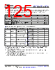
125 / 218 page  6.11.5.7 General Purpose Memory Controller (GPMC) For more details about features and additional description information on the device General-Purpose Memory Controller, see the corresponding subsections within Signal Descriptions and Detailed Description sections. For more information, see the General-Purpose Memory Controller (GPMC) section in the device TRM. 6.11.5.7.1 GPMC Timing Conditions PARAMETER MIN MAX UNIT INPUT CONDITIONS SRI Input Slew Rate 1.65 4 V/ns OUTPUT CONDITIONS CL Output Load Capacitance 3 20 pF PCB CONNECTIVITY REQUIREMENTS td(Trace Delay) Propagation delay of each trace 100MHz 140 720 ps td(Trace Mismatch Delay) Propagation delay mismatch across all traces 200 ps 6.11.5.7.2 GPMC/NOR Flash Timing Requirements - Synchronous Mode 100MHz (1) (2) NO. PARAMETER DESCRIPTION MODE MIN MAX UNIT F12 tsu(dV-clkH) Setup time, GPMC0_AD[31:0] valid before GPMC0_CLK high div_by_1_mode (4) 1.81 ns not_div_by_1_m ode(5) 1.06 ns F13 th(clkH-dV) Hold time, GPMC0_AD[31:0] valid after GPMC0_CLK high div_by_1_mode (4) 2.29 ns not_div_by_1_m ode(5) 2.29 ns F21 tsu(waitV-clkH) Setup time, GPMC0_WAIT[x](3) valid before GPMC0_CLK high div_by_1_mode (4) 1.81 ns not_div_by_1_m ode(5) 1.06 ns F22 th(clkH-waitV) Hold time, GPMC0_WAIT[x](3) valid after GPMC0_CLK high div_by_1_mode (4) 2.29 ns not_div_by_1_m ode(5) 2.29 ns (1) 100MHz GPMC_FCLK selected - CTRLMMR_GPMC_CLKSEL[0] CLK_SEL = 1 = MAIN_PLL2_HSDIV7_CLKOUT (100/60 MHz). (2) Trace length from GPMC pins to device assumed to be less than 4" and length matched to within 200ps for 100MHz Synchronous Mode. (3) In GPMC_WAIT[x], x is equal to 0 or 1. (4) In div_by_1_mode, GPMC0_CLK refers to either GPMC0_CLKOUT or GPMC0_FCLK_MUX (free-running). Both signals are pin- muxed to the same pin. GPMC_CONFIG1_i Register: GPMCFCLKDIVIDER = 0h: – GPMC0_CLK frequency = GPMC_FCLK frequency (5) In not_div_by_1_mode, GPMC_CLK only refers to GPMC0_CLKOUT. GPMC0_FCLK_MUX cannot be clock divided to match the GPMC0_CLKOUT frequency if GPMCFCLKDIVIDER > 0. GPMC_CONFIG1_i Register: GPMCFCLKDIVIDER = 1h to 3h: – GPMC_CLK frequency = GPMC_FCLK frequency / (2 to 4) www.ti.com AM2612, AM2611, AM2611-Q1, AM2612-Q1 SPRSPA7C – SEPTEMBER 2024 – REVISED JULY 2025 Copyright © 2025 Texas Instruments Incorporated Submit Document Feedback 125 Product Folder Links: AM2612 AM2611 AM2611-Q1 AM2612-Q1 |
|
链接网址 |
| ALLDATASHEET是否为您带来帮助? [ DONATE ] |
关于 Alldatasheet | 广告服务 | 联系我们 | 隐私政策 | 数据表链接 | 链接交换 | 制造商名单 All Rights Reserved©Alldatasheet.com |
| Russian : Alldatasheetru.com | Korean : Alldatasheet.co.kr | Spanish : Alldatasheet.es | French : Alldatasheet.fr | Italian : Alldatasheetit.com Portuguese : Alldatasheetpt.com | Polish : Alldatasheet.pl | Vietnamese : Alldatasheet.vn Indian : Alldatasheet.in | Mexican : Alldatasheet.com.mx | British : Alldatasheet.co.uk | New Zealand : Alldatasheet.co.nz |
|
Family Site : ic2ic.com |
icmetro.com |
 Chinese ▼
 English
 Chinese
 German
 Japanese
 Russian
 Korean
 Spanish
 French
 Italian
 Portuguese
 Polish
 Vietnamese
 Indian
 Mexican
 British
 New Zealand