|
数据搜索系统,热门电子元器件搜索 |
|
|
数据搜索系统,热门电子元器件搜索 |
|
M30620FCAFP 数据表(PDF) 421 Page - Renesas Technology Corp |
|
|
|||||||||||||||||||||||||||||
M30620FCAFP 数据表(HTML) 421 Page - Renesas Technology Corp |
|
|
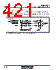
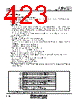
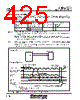
421 / 615 page  Mitsubishi microcomputers M16C / 62A Group SINGLE-CHIP 16-BIT CMOS MICROCOMPUTER 2-104 UART 2.5.7 Error-permitted range range of transfer baud <1ST-8DATA-1SP> ST D0 D7 SP D0 ST D7 SP At the falling edge of ST, the transfer clock is generated, and reception starts. When the transfer rate of the receive data is faster than the rate of the transfer clock on the receiver side RxDi (Receive data) Transfer clock (Receiver side) 1 clock 8 clocks 9.5 clocks ST : Start bit SP : Stop bit ∗ 1 period of BRGi's count source (Maximum) ••• According to the condition of the input timing, a maximum of this period ( ∗) can be omitted. ∗ SP must be detected at this last rising edge of the transfer clock. When the transfer rate of the receive data is slower than the rate of the transfer clock on the receiver side 1 clock During reception, the receive data input to the RXDi pin is taken at the rising edge of the transfer clock. Accordingly, in order to receive data correctly, the stop bit must be input when the transfer clock of one- set receive data rises last. Figure 2.5.21 shows the relationship between the transfer clock and receive data. Figure 2.5.21 Relationship between transfer clock and receive data |
|
链接网址 |
| ALLDATASHEET是否为您带来帮助? [ DONATE ] |
关于 Alldatasheet | 广告服务 | 联系我们 | 隐私政策 | 数据表链接 | 链接交换 | 制造商名单 All Rights Reserved©Alldatasheet.com |
| Russian : Alldatasheetru.com | Korean : Alldatasheet.co.kr | Spanish : Alldatasheet.es | French : Alldatasheet.fr | Italian : Alldatasheetit.com Portuguese : Alldatasheetpt.com | Polish : Alldatasheet.pl | Vietnamese : Alldatasheet.vn Indian : Alldatasheet.in | Mexican : Alldatasheet.com.mx | British : Alldatasheet.co.uk | New Zealand : Alldatasheet.co.nz |
|
Family Site : ic2ic.com |
icmetro.com |
 Chinese ▼
 English
 Chinese
 German
 Japanese
 Russian
 Korean
 Spanish
 French
 Italian
 Portuguese
 Polish
 Vietnamese
 Indian
 Mexican
 British
 New Zealand