|
数据搜索系统,热门电子元器件搜索 |
|
|
数据搜索系统,热门电子元器件搜索 |
|
AD8698ARM-R2 数据表(PDF) 14 Page - Analog Devices |
|
|
|||||||||||||||||||||||||||||
AD8698ARM-R2 数据表(HTML) 14 Page - Analog Devices |
|
|
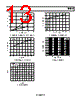
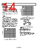
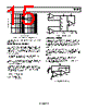
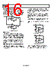
14 / 20 page  AD8698 Rev. 0 | Page 14 of 20 APPLICATIONS INPUT OVERVOLTAGE PROTECTION The AD8698 has internal protective circuitry which allows voltages at either input to exceed the supply voltage. However, if voltages applied at either input exceed the supply voltage by more than 2 V, it is recommended to use a resistor in series with the inputs to limit the input current and prevent damaging the device. The value of the resistor can be calculated from the following formula: mA 5 500 ≤ + − S S IN R V V DRIVING CAPACITIVE LOADS The AD8698 is stable even when driving heavy capacitive loads in any configuration. Although the AD8698 will safely drive capacitive loads well over 10 nF, it is recommended to use external compensation should the amplifier be subjected to driving a load exceeding 50 nF. This is particularly important in positive unity gain configurations, the worst case for stability. Figure 49 shows the output of the AD8698 with a 68 nF load in response to a 400 mV signal at its positive input; the overshoot is less than 25% without any external compensation. Using a simple “snubber” network reduces the overshoot to less than 10% as shown in Figure 50. VS = ±15V CL = 68nF AV = 1 TIME (10 µs/DIV) Figure 49. Heavy Capacitive Load Drive without Compensation VS = ±15V CL = 68nF RS = 30Ω CS = 5nF AV = 1 TIME (10 µs/DIV) Figure 50. Compensated Capacitive Load Drive with Snubber The snubber network consists of a simple RC network whose values are determined empirically. V+ RS CS CL V– 400mV + – Figure 51. Snubber Network Table 5 provides a few starting values for optimum compensation. Table 5. Compensation Values CL (nF) RS ( Ω) CS (nF) 47 20 7 68 30 5 100 50 3 The use of the snubber network does not recover the loss of bandwidth incurred by the load capacitance. The AD8698 maintains a unity gain bandwidth of 1 MHz with load capacitances of up to 1 nF. |
|
|
链接网址 |
| ALLDATASHEET是否为您带来帮助? [ DONATE ] |
关于 Alldatasheet | 广告服务 | 联系我们 | 隐私政策 | 数据表链接 | 链接交换 | 制造商名单 All Rights Reserved©Alldatasheet.com |
| Russian : Alldatasheetru.com | Korean : Alldatasheet.co.kr | Spanish : Alldatasheet.es | French : Alldatasheet.fr | Italian : Alldatasheetit.com Portuguese : Alldatasheetpt.com | Polish : Alldatasheet.pl | Vietnamese : Alldatasheet.vn Indian : Alldatasheet.in | Mexican : Alldatasheet.com.mx | British : Alldatasheet.co.uk | New Zealand : Alldatasheet.co.nz |
|
Family Site : ic2ic.com |
icmetro.com |
 Chinese ▼
 English
 Chinese
 German
 Japanese
 Russian
 Korean
 Spanish
 French
 Italian
 Portuguese
 Polish
 Vietnamese
 Indian
 Mexican
 British
 New Zealand