|
数据搜索系统,热门电子元器件搜索 |
|
|
数据搜索系统,热门电子元器件搜索 |
|
AD8611ARMZ-R2 数据表(PDF) 12 Page - Analog Devices |
|
|
|||||||||||||||||||||||||||||
AD8611ARMZ-R2 数据表(HTML) 12 Page - Analog Devices |
|
|
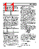
12 / 20 page  AD8611/AD8612 Data Sheet Rev. B | Page 12 of 20 The capacitor CF is optional and can be added to introduce a pole into the feedback network. This has the effect of increasing the amount of hysteresis at high frequencies, which is useful when comparing relatively slow signals in high frequency noise environments. At frequencies greater than fP, the hysteresis window approaches VHI = V+ − 1.5 V and VLO = 0 V. For frequencies less than fP, the threshold voltages remain as in Equation 1. CLOCK TIMING RECOVERY Comparators are often used in digital systems to recover clock timing signals. High speed square waves transmitted over any distance, even tens of centimeters, can become distorted due to stray capacitance and inductance. Poor layout or improper termination can also cause reflections on the transmission line, further distorting the signal waveform. A high speed comparator can recover the distorted waveform while maintaining a minimum of delay. Figure 25 shows VOUT vs. VIN as the AD8611 recovers a 65 MHz, 100 mV peak-to-peak distorted clock signal into a 4 V peak-to- peak square wave. The lower trace is the input to the AD8611, and the upper trace is the QA or QB output from the comparator. The AD8611 is powered from a 5 V single supply. TIME (10ns/DIV) 2V/DIV VOUT VIN 20mV/DIV Figure 25. Using the AD8611 to Recover a Noisy Clock Signal A 5 V, HIGH SPEED WINDOW COMPARATOR A window comparator circuit detects when a signal is between two fixed voltages. The AD8612 can create a high speed window comparator, as shown in Figure 26. In this example, the reference window voltages are set as: 4 3 4 2 1 2 R R R V R R R V LO HI + = + = The output of the A1 comparator goes high when the input signal exceeds VHI, and the output of A2 goes high only when VIN drops below VLO. When the input voltage is between VHI and VLO, both comparator outputs are low, turning off both Q1 and Q2, thus driving VOUT to a high state. If the input signal goes outside of the reference voltage window, VOUT goes low. To ensure a minimum of switching delay, the use of high speed transistors is recommended for Q1 and Q2. Using the AD8612 with 2N3960 transistors provides a total propagation delay from VIN to VOUT of less than 10 ns. Table 8. Window Comparator Output States VOUT Input Voltage ≈ 200 mV VIN < VLO +5 V VLO < VIN < VHI ≈ 200 mV VIN > VHI VHI 5V 5V R1 R2 6 7 3 4 10 1 VIN AD8612 1k Ω VLO 5V R3 R4 9 8 11 5 12 14 AD8612 1k Ω Q1 5V VOUT 1k Ω 500 Ω Q2 500 Ω NOTES 1. Q1, Q2 = 2N3960. 2. PINS 2 AND 13 ARE NO CONNECTS. A1 A2 Figure 26. A High Speed Window Comparator |
|
|
链接网址 |
| ALLDATASHEET是否为您带来帮助? [ DONATE ] |
关于 Alldatasheet | 广告服务 | 联系我们 | 隐私政策 | 数据表链接 | 链接交换 | 制造商名单 All Rights Reserved©Alldatasheet.com |
| Russian : Alldatasheetru.com | Korean : Alldatasheet.co.kr | Spanish : Alldatasheet.es | French : Alldatasheet.fr | Italian : Alldatasheetit.com Portuguese : Alldatasheetpt.com | Polish : Alldatasheet.pl | Vietnamese : Alldatasheet.vn Indian : Alldatasheet.in | Mexican : Alldatasheet.com.mx | British : Alldatasheet.co.uk | New Zealand : Alldatasheet.co.nz |
|
Family Site : ic2ic.com |
icmetro.com |
 Chinese ▼
 English
 Chinese
 German
 Japanese
 Russian
 Korean
 Spanish
 French
 Italian
 Portuguese
 Polish
 Vietnamese
 Indian
 Mexican
 British
 New Zealand