|
数据搜索系统,热门电子元器件搜索 |
|
|
数据搜索系统,热门电子元器件搜索 |
|
ADCMP581BCPZ-R2 数据表(PDF) 14 Page - Analog Devices |
|
|
|||||||||||||||||||||||||||||
ADCMP581BCPZ-R2 数据表(HTML) 14 Page - Analog Devices |
|
|
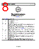
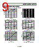
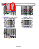
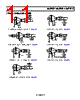
14 / 16 page  ADCMP580/ADCMP581/ADCMP582 Data Sheet Rev. B | Page 14 of 16 COMPARATOR HYSTERESIS Adding hysteresis to a comparator is often desirable in a noisy environment or when the differential inputs are very small or slow moving. The transfer function for a comparator with hystere- sis is shown in Figure 27. If the input voltage approaches the threshold from the negative direction, the comparator switches from a low to a high when the input crosses +VH/2. The new switching threshold becomes −VH/2. The comparator remains in the high state until the threshold −VH/2 is crossed from the positive direction. In this manner, noise centered on 0 V input does not cause the comparator to switch states unless it exceeds the region bounded by ±VH/2. The customary technique for introducing hysteresis into a comparator uses positive feedback from the output back to the input. A limitation of this approach is that the amount of hysteresis varies with the output logic levels, resulting in hysteresis that is not symmetric about the threshold. The external feedback network can also introduce significant parasitics that reduce high speed performance and can even reduce overall stability in some cases. OUTPUT INPUT 0V 0 1 +VH 2 –VH 2 Figure 27. Comparator Hysteresis Transfer Function The ADCMP580/ADCMP581/ADCMP582 family of comparators offers a programmable hysteresis feature that can significantly improve the accuracy and stability of the desired hysteresis. By connecting an external pull-down resistor from the HYS pin to VEE, a variable amount of hysteresis can be applied. Leaving the HYS pin disconnected disables the feature, and hysteresis is then less than 1 mV, as specified. The maximum range of hysteresis that can be applied by using this method is approximately ±70 mV. Figure 28 illustrates the amount of applied hysteresis as a function of the external resistor value. The advantage of applying hysteresis in this manner is improved accuracy, stability, and reduced component count. An external bypass capacitor is not required on the HYS pin, and it would likely degrade the jitter performance of the device. The hysteresis pin can also be driven by a current source. It is biased approximately 400 mV above VEE and has an internal series resistance of approximately 600 Ω. 80 0 1 10k RHYS CONTROL RESISTOR (Ω) 70 60 50 40 30 20 10 10 100 1k Figure 28. Comparator Hysteresis vs. RHYS Control Resistor MINIMUM INPUT SLEW RATE REQUIREMENT As with many high speed comparators, a minimum slew rate requirement must be met to ensure that the device does not oscillate as the input signal crosses the threshold. This oscil- lation is due in part to the high input bandwidth of the comparator and the feedback parasitics inherent in the package. A minimum slew rate of 50 V/µs must ensure clean output transitions from the ADCMP580/ADCMP581/ADCMP582 family of comparators. The slew rate may be too slow for other reasons. The extremely high bandwidth of these devices means that broadband noise can be a significant factor when input slew rates are low. There is 120 μV of thermal noise generated over the bandwidth of the comparator by the two 50 Ω terminations at room temperature. With a slew rate of only 50 V/μs, the inputs are inside this noise band for over 2 ps, rendering the comparator’s jitter performance of 200 fs irrelevant. Raising the slew rate of the input signal and/or reducing the bandwidth over which that resistance is seen at the input can greatly reduce jitter. Devices are not characterized this way but simply bypassing a reference input close to the package can reduce jitter 30% in low slew rate applications. |
|
|
链接网址 |
| ALLDATASHEET是否为您带来帮助? [ DONATE ] |
关于 Alldatasheet | 广告服务 | 联系我们 | 隐私政策 | 数据表链接 | 链接交换 | 制造商名单 All Rights Reserved©Alldatasheet.com |
| Russian : Alldatasheetru.com | Korean : Alldatasheet.co.kr | Spanish : Alldatasheet.es | French : Alldatasheet.fr | Italian : Alldatasheetit.com Portuguese : Alldatasheetpt.com | Polish : Alldatasheet.pl | Vietnamese : Alldatasheet.vn Indian : Alldatasheet.in | Mexican : Alldatasheet.com.mx | British : Alldatasheet.co.uk | New Zealand : Alldatasheet.co.nz |
|
Family Site : ic2ic.com |
icmetro.com |
 Chinese ▼
 English
 Chinese
 German
 Japanese
 Russian
 Korean
 Spanish
 French
 Italian
 Portuguese
 Polish
 Vietnamese
 Indian
 Mexican
 British
 New Zealand