|
数据搜索系统,热门电子元器件搜索 |
|
|
数据搜索系统,热门电子元器件搜索 |
|
FP1108R1-R15-R 数据表(PDF) 2 Page - Eaton All Rights Reserved. |
|
|
|||||||||||||||||||||||||||||
FP1108R1-R15-R 数据表(HTML) 2 Page - Eaton All Rights Reserved. |
|
|
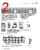
2 / 4 page  2 Technical Data 10227 Effective September 2017 FP1108R High frequency, high current power inductors www.eaton.com/electronics Dimensions - mm Product specifications 1. Open Circuit Inductance (OCL) Test Parameters: 100 kHz, 0.1 V rms, 0.0 Adc, +25 °C 2. Full Load Inductance (FLL) Test Parameters: 100 kHz, 0.1 V rms, Isat1, +25 °C 3. I rms: DC current for an approximate temperature rise of 40 °C without core loss. Derating is necessary for AC currents. PCB layout, trace thickness and width, air-flow, and proximity of other heat generating components will affect the temperature rise. It is recommended that the temperature of the part not exceed +125 °C under worst case operating conditions verified in the end application. 4. I sat1 : Peak current for approximately 20% (R10 10%) rolloff @ +25 °C (R10 10%) 5. I sat2: Peak current for approximately 20% (R10 10%) rolloff @ +85 °C 6. Isat3 : Peak current for approximately 20% (R10 10%) rolloff @ +100 °C 7. Isat4: Peak current for approximately 20% (R10 10%) rolloff @ +125 °C 8. K-factor: Used to determine B p-p for core loss (see graph). Bp-p = K * L * ∆I. B p-p:(Gauss), K: (K-factor from table), L: (Inductance in µH), ∆I (peak to peak ripple current in amps). 9. Part Number Definition: FP1108Rx-yyy-R - FP1108Rx = Product code and size - Rx = DCR indicator - yyy= Inductance value in µH - “-R” suffix = RoHS compliant Part Number9 OCL1 (nH) ±10% FLL min.2 (nH) I rms 3 (A) I sat1 4 (A) I sat2 5 (A) I sat3 6 (A) I sat4 7 (A) DCR (mΩ) @ +20 °C K-factor8 FP1108R1-R10-R 100 81 65 100+ 96 94 90 0.29±5% 330 FP1108R1-R15-R 150 110 77 72 66 63 330 FP1108R1-R18-R 180 132 65 61 58 50 330 FP1108R1-R21-R 210 151 55 51 48 45 330 DCR measured from point “A” to point “B” Part marking: FP1108R1 (Product code and size), xxx = Inductance value in µH, wwllyy= date code, R= revision level Tolerances are ±0.15 millimeters unless stated otherwise PCB tolerances are ±0.1millimeters unless otherwise specified. All soldering surfaces to be be coplanar within 0.1 millimeters. Termination finish: matte Sn with Ni underplate Do not route traces or vias underneath inductor Top View Side View Bottom View Recommended Pad Layout Schematic 7.7 B 2.1 +0.3/-0.2 ±0.2 FP1108R1 0.2 xxx 10.7 typ. 6.7 11.4 wwllyy R ±0.3 typ. 2.0 ±0.2 3.10 (2x) A 2.50 (2x) Front View 7.5 max Packaging information - mm 1.5 dia 1.75 4.0 A 2.0 11.5 FP1108R1 24 xxx ±0.3 11.2 wwllyy R 7.7 16.0 A 8.2 1.5 dia User Direction of Feed Section A-A Supplied in tape and reel packaging, 500 parts per 13” diameter reel, |
|
|
链接网址 |
| ALLDATASHEET是否为您带来帮助? [ DONATE ] |
关于 Alldatasheet | 广告服务 | 联系我们 | 隐私政策 | 数据表链接 | 链接交换 | 制造商名单 All Rights Reserved©Alldatasheet.com |
| Russian : Alldatasheetru.com | Korean : Alldatasheet.co.kr | Spanish : Alldatasheet.es | French : Alldatasheet.fr | Italian : Alldatasheetit.com Portuguese : Alldatasheetpt.com | Polish : Alldatasheet.pl | Vietnamese : Alldatasheet.vn Indian : Alldatasheet.in | Mexican : Alldatasheet.com.mx | British : Alldatasheet.co.uk | New Zealand : Alldatasheet.co.nz |
|
Family Site : ic2ic.com |
icmetro.com |
 Chinese ▼
 English
 Chinese
 German
 Japanese
 Russian
 Korean
 Spanish
 French
 Italian
 Portuguese
 Polish
 Vietnamese
 Indian
 Mexican
 British
 New Zealand