SPT
2
6/24/97
SPT1175
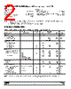
ELECTRICAL SPECIFICATIONS
TA= +25 °C, AVDD=DVDD=+5.0 V, AGND=DGND=0.0 V, VRB=+0.6 V and VRT=+2.6 V, unless otherwise specified.
TEST
TEST
SPT1175
PARAMETERS
CONDITIONS
LEVEL
MIN
TYP
MAX
UNITS
Resolution
8
Bits
DC Accuracy (+25
°C)
Integral Nonlinearity
I
±0.8
±1.2
LSB
Differential Nonlinearity
I
±0.6
±1.0
LSB
No Missing Codes
I
Guaranteed
Analog Input
Input Voltage Range
I
VRB
VRT
V
Input Bias Current
I
±5.0
µA
Input Resistance
VI
100
200
k
Ω
Input Capacitance
V
15
pF
Input Bandwidth
V
12
MHz
Reference Input
Reference Ladder Resistance
I
200
300
400
Ω
Reference Current
I
5.0
6.7
10.0
mA
Reference Input Voltage
VRB
IV
0
0.6
-
V
VRT
IV
-
2.6
2.8
V
Internal Bias
VRB
I
0.55
0.60
0.65
V
VRT-VRB
I
1.9
2.0
2.1
V
Short VRT and VRTS
Short VRB and VRBS
Offset Voltage Error
Top
I
-18
-25
-68
mV
Bottom
I
0
10
40
mV
Timing Characteristics
Maximum Conversion Rate
1 MHz Input Sine Wave
I
20
30
MSPS
Output Data Delay (td)
IV
18
30
ns
Output Data Delay
(High Z)
IV
100
ns
(Tdish, Tdisl)
Data Valid Time
Tri-State Circuit
IV
100
ns
(Teneh, Tenel)
Sampling Time Offset
IV
5
10
ns
ABSOLUTE MAXIMUM RATINGS (Beyond which damage may occur)(1) 25
°C
Supply Voltages
VDD ........................................................... -0.5 to +7.0 V
Input Voltages
Analog Input .............................................. AGND to VDD
Reference Input Voltage ........................... AGND to VDD
ESD Susceptibility(2) .................................................
±1,500 V
Temperature
Operating Temperature ................................. 0 to +70
°C
Junction Temperature ........................................... 175
°C
Lead Temperature, (soldering 10 seconds) .......... 300
°C
Storage Temperature ................................ -55 to +125
°C
Notes: 1.
Operation at any Absolute Maximum Rating is not implied. See Electrical Specifications for proper nominal
applied conditions in typical applications.
2.
100 pF discharged through a 1.5 k
Ω resistor (human body model).
NOTE: It is strongly recommended that all of the supply pins (AVDD, DVDD) be powered from the same source.

 Chinese ▼
 English
 Chinese
 German
 Japanese
 Russian
 Korean
 Spanish
 French
 Italian
 Portuguese
 Polish
 Vietnamese
 Indian
 Mexican
 British
 New Zealand