|
数据搜索系统,热门电子元器件搜索 |
|
|
数据搜索系统,热门电子元器件搜索 |
|
LM393DRE4 数据表(PDF) 11 Page - Texas Instruments |
|
|
|
|||||||||||||||||||||||||||||
LM393DRE4 数据表(HTML) 11 Page - Texas Instruments |
|
|
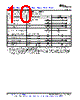
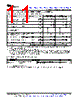
11 / 46 page  11 LM193, LM293, LM293A, LM393, LM393A, LM2903, LM2903V, LM393B, LM2903B www.ti.com SLCS005AB – OCTOBER 1979 – REVISED DECEMBER 2019 Product Folder Links: LM193 LM293 LM293A LM393 LM393A LM2903 LM2903V LM393B LM2903B Submit Documentation Feedback Copyright © 1979–2019, Texas Instruments Incorporated (1) Full range (minimum or maximum) for LM2903 is –40°C to 125°C. All characteristics are measured with zero common-mode input voltage, unless otherwise specified. (2) VCC MAX = 30 V for non-V devices and 32 V for V-suffix devices. (3) The voltage at either input should not be allowed to go negative by more than 0.3 V otherwise output may be incorrect and excessive input current can flow. The upper end of the common-mode voltage range is limited by VCC – 2V. However only one input needs to be in the valid common mode range, the other input can go up the maximum VCC level and the comparator provides a proper output state. Either or both inputs can go to maximum VCC level without damage. 6.12 Electrical Characteristics for LM2903, LM2903V, and LM2903AV at specified free-air temperature, VCC = 5 V (unless otherwise noted) PARAMETER TEST CONDITIONS TA (1) LM2903, LM2903V LM2903AV UNIT MIN TYP MAX MIN TYP MAX VIO Input offset voltage VCC = 5 V to MAX (2) , VO = 1.4 V, VIC = VICR(min), 25°C 2 7 1 2 mV Full range 15 4 IIO Input offset current VO = 1.4 V 25°C 5 50 5 50 nA Full range 200 200 IIB Input bias current VO = 1.4 V 25°C –25 –250 –25 –250 nA Full range –500 –500 VICR Common-mode input- voltage range(3) 25°C 0 to VCC – 1.5 0 to VCC – 1.5 V Full range 0 to VCC – 2 0 to VCC – 2 AVD Large-signal differential- voltage amplification VCC = 15 V, VO = 1.4 V to 11.4 V, RL ≥ 15 kΩ to VCC 25°C 25 100 25 100 V/mV IOH High-level output current VOH = 5 V, VID = 1 V 25°C 0.1 50 0.1 50 nA VOH = VCC MAX (2), VID = 1 V Full range 1 1 µA VOL Low-level output voltage IOL = 4 mA, VID = –1 V, 25°C 150 400 150 400 mV Full range 700 700 IOL Low-level output current VOL = 1.5 V, VID = –1 V 25°C 6 6 mA ICC Supply current RL = ∞ VCC = 5 V 25°C 0.8 1 0.8 1 mA VCC = MAX Full range 2.5 2.5 (1) CL includes probe and jig capacitance. (2) The response time specified is the interval between the input step function and the instant when the output crosses 1.4 V. 6.13 Switching Characteristics (all devices) VCC = 5 V, TA = 25°C PARAMETER TEST CONDITIONS TYP UNIT Response time RL connected to 5 V through 5.1 kΩ, CL = 15 pF (1) (2) 100-mV input step with 5-mV overdrive 1.3 µs TTL-level input step 0.3 |
|
链接网址 |
| ALLDATASHEET是否为您带来帮助? [ DONATE ] |
关于 Alldatasheet | 广告服务 | 联系我们 | 隐私政策 | 数据表链接 | 链接交换 | 制造商名单 All Rights Reserved©Alldatasheet.com |
| Russian : Alldatasheetru.com | Korean : Alldatasheet.co.kr | Spanish : Alldatasheet.es | French : Alldatasheet.fr | Italian : Alldatasheetit.com Portuguese : Alldatasheetpt.com | Polish : Alldatasheet.pl | Vietnamese : Alldatasheet.vn Indian : Alldatasheet.in | Mexican : Alldatasheet.com.mx | British : Alldatasheet.co.uk | New Zealand : Alldatasheet.co.nz |
|
Family Site : ic2ic.com |
icmetro.com |
 Chinese ▼
 English
 Chinese
 German
 Japanese
 Russian
 Korean
 Spanish
 French
 Italian
 Portuguese
 Polish
 Vietnamese
 Indian
 Mexican
 British
 New Zealand