|
数据搜索系统,热门电子元器件搜索 |
|
|
数据搜索系统,热门电子元器件搜索 |
|
SN74LS393D 数据表(PDF) 2 Page - ON Semiconductor |
|
|
|||||||||||||||||||||||||||||
SN74LS393D 数据表(HTML) 2 Page - ON Semiconductor |
|
|
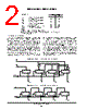
2 / 5 page  5-2 FAST AND LS TTL DATA SN54/74LS390 • SN54/74LS393 PIN NAMES LOADING (Note a) HIGH LOW CP Clock (Active LOW going edge) Input to +16 (LS393) 0.5 U.L. 1.0 U.L. CP0 Clock (Active LOW going edge) Input to ÷2 (LS390) 0.5 U.L. 1.0 U.L. CP1 Clock (Active LOW going edge) Input to ÷5 (LS390) 0.5 U.L. 1.5 U.L. MR Master Reset (Active HIGH) Input 0.5 U.L. 0.25 U.L. Q0 –Q3 Flip-Flop outputs (Note b) 10 U.L. 5 (2.5) U.L. NOTES: a) 1 TTL Unit Load (U.L.) = 40 µA HIGH/1.6 mA LOW. b) The Output LOW drive factor is 2.5 U.L. for Military (54) and 5 U.L. for Commercial (74) b) Temperature Ranges. FUNCTIONAL DESCRIPTION Each half of the SN54 / 74LS393 operates in the Modulo 16 binary sequence, as indicated in the ÷16 Truth Table. The first flip-flop is triggered by HIGH-to-LOW transitions of the CP input signal. Each of the other flip-flops is triggered by a HIGH-to-LOW transition of the Q output of the preceding flip-flop. Thus state changes of the Q outputs do not occur simultaneously. This means that logic signals derived from combinations of these outputs will be subject to decoding spikes and, therefore, should not be used as clocks for other counters, registers or flip-flops. A HIGH signal on MR forces all outputs to the LOW state and prevents counting. Each half of the LS390 contains a ÷5 section that is independent except for the common MR function. The ÷5 section operates in 4.2.1 binary sequence, as shown in the ÷5 Truth Table, with the third stage output exhibiting a 20% duty cycle when the input frequency is constant. To obtain a ÷10 function having a 50% duty cycle output, connect the input signal to CP1 and connect the Q3 output to the CP0 input; the Q0 output provides the desired 50% duty cycle output. If the input frequency is connected to CP0 and the Q0 output is connected to CP1, a decade divider operating in the 8.4.2.1 BCD code is obtained, as shown in the BCD Truth Table. Since the flip-flops change state asynchronously, logic signals derived from combinations of LS390 outputs are also subject to decoding spikes. A HIGH signal on MR forces all outputs LOW and prevents counting. SN54 / 74LS390 LOGIC DIAGRAM (one half shown) SN54 / 74LS393 LOGIC DIAGRAM (one half shown) CP1 CP0 MR MR CP KCP J CD Q KCP J CD Q KCP J CD Q KCP J CD Q KCP J CD Q KCP J CD Q KCP J CD Q KCP J CD Q Q0 Q0 Q1 Q1 Q2 Q2 Q3 Q3 |
|
|
链接网址 |
| ALLDATASHEET是否为您带来帮助? [ DONATE ] |
关于 Alldatasheet | 广告服务 | 联系我们 | 隐私政策 | 数据表链接 | 链接交换 | 制造商名单 All Rights Reserved©Alldatasheet.com |
| Russian : Alldatasheetru.com | Korean : Alldatasheet.co.kr | Spanish : Alldatasheet.es | French : Alldatasheet.fr | Italian : Alldatasheetit.com Portuguese : Alldatasheetpt.com | Polish : Alldatasheet.pl | Vietnamese : Alldatasheet.vn Indian : Alldatasheet.in | Mexican : Alldatasheet.com.mx | British : Alldatasheet.co.uk | New Zealand : Alldatasheet.co.nz |
|
Family Site : ic2ic.com |
icmetro.com |
 Chinese ▼
 English
 Chinese
 German
 Japanese
 Russian
 Korean
 Spanish
 French
 Italian
 Portuguese
 Polish
 Vietnamese
 Indian
 Mexican
 British
 New Zealand