|
数据搜索系统,热门电子元器件搜索 |
|
|
数据搜索系统,热门电子元器件搜索 |
|
PIP3206-R 数据表(PDF) 2 Page - NXP Semiconductors |
|
|
|||||||||||||||||||||||||||||
PIP3206-R 数据表(HTML) 2 Page - NXP Semiconductors |
|
|
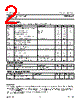
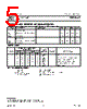
2 / 8 page  Philips Semiconductors Preliminary specification TOPFET high side switch PIP3206-R SMD version LIMITING VALUES Limiting values in accordance with the Absolute Maximum System (IEC 134) SYMBOL PARAMETER CONDITIONS MIN. MAX. UNIT V BG Continuous off-state supply voltage 0 50 V I L Continuous load current T mb ≤ 140˚C - 10 A P D Total power dissipation T mb ≤ 25˚C - 115 W T stg Storage temperature -55 175 ˚C T j Continuous junction temperature 1 - 150 ˚C T sold Mounting base temperature during soldering - 260 ˚C Reverse battery voltages 2 -V BG Continuous reverse voltage - 16 V -V BG Peak reverse voltage - 32 V Application information R I, RS External resistors 3 to limit input, status currents 3.2 - k Ω Input and status I I, IS Continuous currents -5 5 mA I I, IS Repetitive peak currents δ ≤ 0.1, tp = 300 µs -50 50 mA Inductive load clamping I L = 10 A, VBG = 16 V E BL Non-repetitive clamping energy T j = 150˚C prior to turn-off - 460 mJ ESD LIMITING VALUE SYMBOL PARAMETER CONDITIONS MIN. MAX. UNIT V C Electrostatic discharge capacitor Human body model; - 2 kV voltage C = 250 pF; R = 1.5 k Ω THERMAL CHARACTERISTICS SYMBOL PARAMETER CONDITIONS MIN. TYP. MAX. UNIT Thermal resistance 4 R th j-mb Junction to mounting base - - 0.86 1.08 K/W 1 For normal continuous operation. A higher T j is allowed as an overload condition but at the threshold Tj(TO) the over temperature trip operates to protect the switch. 2 Reverse battery voltage is allowed only with external resistors to limit the input and status currents to a safe value. The connected load must limit the reverse load current. The internal ground resistor limits the reverse battery ground current. Power is dissipated and the T j rating must be observed. 3 To limit currents during reverse battery and transient overvoltages (positive or negative). 4 Of the output power MOS transistor. October 2001 2 Rev 1.000 |
|
|
链接网址 |
| ALLDATASHEET是否为您带来帮助? [ DONATE ] |
关于 Alldatasheet | 广告服务 | 联系我们 | 隐私政策 | 数据表链接 | 链接交换 | 制造商名单 All Rights Reserved©Alldatasheet.com |
| Russian : Alldatasheetru.com | Korean : Alldatasheet.co.kr | Spanish : Alldatasheet.es | French : Alldatasheet.fr | Italian : Alldatasheetit.com Portuguese : Alldatasheetpt.com | Polish : Alldatasheet.pl | Vietnamese : Alldatasheet.vn Indian : Alldatasheet.in | Mexican : Alldatasheet.com.mx | British : Alldatasheet.co.uk | New Zealand : Alldatasheet.co.nz |
|
Family Site : ic2ic.com |
icmetro.com |
 Chinese ▼
 English
 Chinese
 German
 Japanese
 Russian
 Korean
 Spanish
 French
 Italian
 Portuguese
 Polish
 Vietnamese
 Indian
 Mexican
 British
 New Zealand