|
数据搜索系统,热门电子元器件搜索 |
|
|
数据搜索系统,热门电子元器件搜索 |
|
PLL702-06SC-R 数据表(PDF) 3 Page - PhaseLink Corporation |
|
|
|||||||||||||||||||||||||||||
PLL702-06SC-R 数据表(HTML) 3 Page - PhaseLink Corporation |
|
|
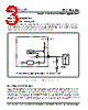
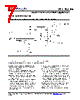
3 / 8 page  PLL702-06 Clock Generator for Printer Applications 47745 Fremont Blvd., Fremont, California 94538 Tel (510) 492-0990 Fax (510) 492-0991 www.phaselink.com Rev 10/26/05 Page 3 FUNCTIONAL DESCRIPTION Tri-level and two-level inputs In order to reduce pin usage, the PLL702-06 uses tri-level input pins. These pins allow 3 levels for input selection: namely, 0 = Connect to GND, 1 = Connect to VDD, M = Do not connect. Thus, unlike the two-level selection pins, the tri-level input pins are in the “M” (mid) state when not connected. In order to connect a tri-level pin to a logical “zero”, the pin must be connected to GND. Likewise, in order to connect to a logical “one”, the pin must be connected to VDD. BI-DIRECTIONAL PINS WITH INTERNAL PULL-UP Connecting a bi-directional pin The PLL702-06 also uses bi-directional pins. The same pin serves as input upon power-up, and as output as soon as the inputs have been latched. The value of the input is latched-in upon power-up. Depending on the pin (see pin description), the input can be tri-level or a standard two-level. Unlike unidirectional pins, bi-directional pins cannot be connected directly to GND or VDD in order to set the input to "0" or "1", since the pin also needs to serve as output. In the case of two level input pins, an internal pull- up resistor is present. This allows a default value to be set when no external pull down resistor is connected between the pin and GND (by definition, a tri-level input has a default value of "M" (mid) if it is not connected). In order to connect a bi-directional pin to a non-default value, the input must be connected to GND or VDD through an external pull-down/pull-up resistor. Latch Power Up Reset Jumper options R UP/4 Clock Load Latched Input Output EN VDD R up Bi-directional pin R RB NOTE: Rup=Internal pull-up resistor (see pin description). Power-up Reset : R starts from 1 to 0 while RB starts from 0 to 1. Internal to chip External Circuitry |
|
|
链接网址 |
| ALLDATASHEET是否为您带来帮助? [ DONATE ] |
关于 Alldatasheet | 广告服务 | 联系我们 | 隐私政策 | 数据表链接 | 链接交换 | 制造商名单 All Rights Reserved©Alldatasheet.com |
| Russian : Alldatasheetru.com | Korean : Alldatasheet.co.kr | Spanish : Alldatasheet.es | French : Alldatasheet.fr | Italian : Alldatasheetit.com Portuguese : Alldatasheetpt.com | Polish : Alldatasheet.pl | Vietnamese : Alldatasheet.vn Indian : Alldatasheet.in | Mexican : Alldatasheet.com.mx | British : Alldatasheet.co.uk | New Zealand : Alldatasheet.co.nz |
|
Family Site : ic2ic.com |
icmetro.com |
 Chinese ▼
 English
 Chinese
 German
 Japanese
 Russian
 Korean
 Spanish
 French
 Italian
 Portuguese
 Polish
 Vietnamese
 Indian
 Mexican
 British
 New Zealand