|
数据搜索系统,热门电子元器件搜索 |
|
|
数据搜索系统,热门电子元器件搜索 |
|
DFE201612E-R33M 数据表(PDF) 9 Page - Analog Devices |
|
|
|||||||||||||||||||||||||||||
DFE201612E-R33M 数据表(HTML) 9 Page - Analog Devices |
|
|
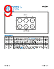
9 / 17 page  500mV to 5.5V Input, Ultrasonic Boost Converter with Short-Circuit Protection and True Shutdown MAX18002 www.analog.com Analog Devices | 9 Pin Configuration LX IN EN RSEL GND OUT A B 1 2 3 TOP VIEW (BUMP SIDE DOWN) MAX18002 + 6 WLP (1.07mm x 1.57mm x 0.5mm) Pin Description PIN NAME FUNCTION Type A1 LX Switching Node. Connect the inductor (See the Inductor Selection section for more information) from LX to IN. Power A2 IN Input Pin. Connect a 22μF X7R ceramic capacitor from IN to ground. Depending on the specific application requirements, more capacitance may be needed. Power A3 EN Enable Input Pin. Force this pin to higher than 1.2V to enable the boost converter. Force this pin below 0.4V to disable the part and enter True Shutdown mode. Digital B1 OUT Output Pin. Connect a 2 x 22μF X7R ceramic capacitor from OUT to GND. Power B2 PGND Power Ground. Connect to System GND Ground B3 RSEL Output Voltage Select Pin. Connect a resistor from RSEL to GND based on the desired output voltages. See Table 1 for more information. RSEL floats in shutdown. Care must be taken that the total capacitance on this pin should be less than 2pF. Analog |
|
|
链接网址 |
| ALLDATASHEET是否为您带来帮助? [ DONATE ] |
关于 Alldatasheet | 广告服务 | 联系我们 | 隐私政策 | 数据表链接 | 链接交换 | 制造商名单 All Rights Reserved©Alldatasheet.com |
| Russian : Alldatasheetru.com | Korean : Alldatasheet.co.kr | Spanish : Alldatasheet.es | French : Alldatasheet.fr | Italian : Alldatasheetit.com Portuguese : Alldatasheetpt.com | Polish : Alldatasheet.pl | Vietnamese : Alldatasheet.vn Indian : Alldatasheet.in | Mexican : Alldatasheet.com.mx | British : Alldatasheet.co.uk | New Zealand : Alldatasheet.co.nz |
|
Family Site : ic2ic.com |
icmetro.com |
 Chinese ▼
 English
 Chinese
 German
 Japanese
 Russian
 Korean
 Spanish
 French
 Italian
 Portuguese
 Polish
 Vietnamese
 Indian
 Mexican
 British
 New Zealand