|
数据搜索系统,热门电子元器件搜索 |
|
|
数据搜索系统,热门电子元器件搜索 |
|
P9027LP-R 数据表(PDF) 14 Page - Renesas Technology Corp |
|
|
|||||||||||||||||||||||||||||
P9027LP-R 数据表(HTML) 14 Page - Renesas Technology Corp |
|
|
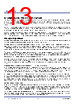
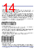
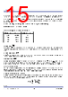
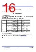
14 / 28 page  P9027LP-R Datasheet © 2016 Integrated Device Technology, Inc 14 April 28, 2016 Charge Pump for Internal Power Supply - VDD The power supply for the control circuitry in the P9027LP-R is generated by a charge pump. This charge pump requires a 0.47 µF flying capacitor connected between the CFLY1 and CFLY2 terminals. A 1 µF capacitor with a recommended voltage rating of 25 V must be connected from VDD to GND. Adding any external loads to this pin is prohibited as the charge pump output current is limited to 5 mA. Rectifier Voltage Headroom Setting – VHDR The rectifier voltage dynamically changes as a function of load when the VHDR resistor is fixed. The reason is to balance power dissipation and dynamic load response. Under the condition of a step load, the wireless power system may not have enough power to respond. This is due to the communication of the Rx-to-Tx feedback loop being relatively slow – where it can take up to several tens of milliseconds for the power required by the receiver to be delivered. Thus, a higher rectifier voltage is preferred to mitigate the step load transient response. On the other hand, a high rectifier voltage will generate more power loss on the LDO. Thus, to meet the requirements of both power dissipation and transient response, the rectifier voltage typically starts at around 6.5V at no load, and it is adjusted to the appropriate value based on the output load once the communication is complete. Figure 11 shows how the rectifier voltage changes with load. The rectifier voltage is set by connecting a 1% resistor from the VHDR pin to GND. The table below recommends the appropriate resistor value based on system efficiency and transient response when using P9235A-R and P9027LP-R. Table 6. Resistor Value and Output Current Resistor Value ( KΩ ) Output Current 1.13 0 – 400mA 1.69 400 – 600mA Rectifier Voltage - RECT The rectifier output (RECT pin) requires at least a 20 μF ceramic capacitor from the pin to GND to minimize the ripple voltage. It is recommended to use at least either two 10 μF or four 4.7 μF capacitors to reduce the total capacitor ESR. When selecting a ceramic capacitor, only X5R and X7R dielectric types should be used. Other types such as Z5U and Y5F have such severe loss of capacitance due to effects of temperature variation and applied voltage, they may provide as little as 20% of rated capacitance in many typical applications. Always consult the capacitor manufacturer’s data curves before selecting a capacitor. Setting the Output Voltage - VSET The P9027LP-R output voltage can be programmed from 4.5 to 6.0 V by connecting a resistor from the VSET pin to GNDx allowing selection from pre-programmed voltages. See the table below for the desired output voltage with an appropriate resistor value. Table 7. Resistor Value and Output Voltage Resistor Value ( KΩ ) Output Voltage 3.40 4.50 4.22 4.75 GND 5.00 5.36 5.25 6.49 5.50 7.68 5.75 9.09 6.00 Over-Current Limit – IOC The output over-current (OC) protection mechanism relies on the comparison between the sensed current and the programmed over-current threshold. The over-current threshold is set through a single external resistor, connected between the IOC pin and GND. A pulse 100 µA of current is sourced from the IOC pin to GND. If IOC pin is shorted to GND, the protection is disabled. The LDO output current sensing is |
|
|
链接网址 |
| ALLDATASHEET是否为您带来帮助? [ DONATE ] |
关于 Alldatasheet | 广告服务 | 联系我们 | 隐私政策 | 数据表链接 | 链接交换 | 制造商名单 All Rights Reserved©Alldatasheet.com |
| Russian : Alldatasheetru.com | Korean : Alldatasheet.co.kr | Spanish : Alldatasheet.es | French : Alldatasheet.fr | Italian : Alldatasheetit.com Portuguese : Alldatasheetpt.com | Polish : Alldatasheet.pl | Vietnamese : Alldatasheet.vn Indian : Alldatasheet.in | Mexican : Alldatasheet.com.mx | British : Alldatasheet.co.uk | New Zealand : Alldatasheet.co.nz |
|
Family Site : ic2ic.com |
icmetro.com |
 Chinese ▼
 English
 Chinese
 German
 Japanese
 Russian
 Korean
 Spanish
 French
 Italian
 Portuguese
 Polish
 Vietnamese
 Indian
 Mexican
 British
 New Zealand