|
数据搜索系统,热门电子元器件搜索 |
|
|
数据搜索系统,热门电子元器件搜索 |
|
ADCA3280ACEZ-R7 数据表(PDF) 13 Page - Analog Devices |
|
|
|||||||||||||||||||||||||||||
ADCA3280ACEZ-R7 数据表(HTML) 13 Page - Analog Devices |
|
|
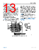
13 / 18 page  Data Sheet ADCA3280 APPLICATIONS INFORMATION analog.com Rev. 0 | 13 of 18 THERMAL CONSIDERATIONS The ADCA3280 is packaged in an industry-standard 9-terminal, 9 mm x 8 mm LGA_CAV package. The thermal resistance from θJC is 3.2°C/W at 24 V, where the case is defined by the exposed pad on the bottom of the package. For the best thermal performance, it is recommended to add as many thermal vias as possible under the exposed pad of the LGA_CAV. Thermal transfer is maximized when the amount of copper under the exposed pad is maximized. A solid copper slug captured in the PCB can also be used in place of vias to provide additional thermal benefits; however, this slug is not required for typical operation. The array of vias under the ADCA3280 must interface to an external heat sink such as a pedestal on the system chassis. SOLDERING INFORMATION AND RECOMMENDED PCB LAND PATTERN Figure 22 shows the recommended land pattern for the ADCA3280. To minimize thermal impedance, the exposed pad on the 9 mm × 8 mm LGA_CAV is soldered to a ground plane. To improve thermal dissipation, 188 thermal vias are arranged in an array under the exposed pad. The array consists of alternating rows of 13 vias and 12 vias, maximizing the number of vias within the area. The area under the exposed pad is also tied to ground on the bottom layer of the PCB. If multiple ground layers exist, tie these layers together by the vias. The external layer of the PCB must be a minimum of 1 oz. copper. The minimum average plated hole wall thickness of the vias must not be less than 0.001 inches. Additional copper and vias extending beyond the top and bottom of the ADCA3280 package can provide a small additional thermal benefit. Figure 23 shows the recommended solder dispense pattern for the ADCA3280. The pads are fully covered with solder, while the thermal pad has 40% coverage broken into squares to minimize solder voiding. For further information on optimizing the thermal performance while using the ADCA3280, refer to the AN-1604 Application Note, Ther- mal Management Calculations for RF Amplifiers in LFCSP and Flange Packages. Figure 22. Recommended PCB Layout (Dimensions Shown in Millimeters) |
|
|
链接网址 |
| ALLDATASHEET是否为您带来帮助? [ DONATE ] |
关于 Alldatasheet | 广告服务 | 联系我们 | 隐私政策 | 数据表链接 | 链接交换 | 制造商名单 All Rights Reserved©Alldatasheet.com |
| Russian : Alldatasheetru.com | Korean : Alldatasheet.co.kr | Spanish : Alldatasheet.es | French : Alldatasheet.fr | Italian : Alldatasheetit.com Portuguese : Alldatasheetpt.com | Polish : Alldatasheet.pl | Vietnamese : Alldatasheet.vn Indian : Alldatasheet.in | Mexican : Alldatasheet.com.mx | British : Alldatasheet.co.uk | New Zealand : Alldatasheet.co.nz |
|
Family Site : ic2ic.com |
icmetro.com |
 Chinese ▼
 English
 Chinese
 German
 Japanese
 Russian
 Korean
 Spanish
 French
 Italian
 Portuguese
 Polish
 Vietnamese
 Indian
 Mexican
 British
 New Zealand