|
数据搜索系统,热门电子元器件搜索 |
|
|
数据搜索系统,热门电子元器件搜索 |
|
UPC1663 数据表(PDF) 4 Page - Renesas Technology Corp |
|
|
|||||||||||||||||||||||||||||
UPC1663 数据表(HTML) 4 Page - Renesas Technology Corp |
|
|
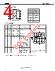
4 / 18 page  Data Sheet G11024EJ6V0DS00 2 µµµµPC1663 CONNECTION DIAGRAM PIN EXPLANATIONS Pin No. Pin Name In Dual Bias (V) In Single Bias (V) Functions and Applications Internal Equivalent Circuit 8 1 IN1 IN2 Pin voltage 0 Apply voltage VCC/2 Input pin 5 4 OUT1 OUT2 Pin voltage 0 Apply voltage VCC/2 Output pin 6VCC + ±2 to ±6.5 –0.3 to +14 Plus voltage supply pin. This pin should be connected with bypass capacitor to minimize AC impedance. 3VCC – GND Minus voltage supply pin. This pin should be connected with bypass capacitor to minimize AC impedance. 7 2 G1A G1B — — Gain adjustment pin. External resistor from 0 to 10 k Ω can be inserted between pin 2 and 7 to determine gain value. (G2A)(G2B) Note Note 8 1 7 2 6 5 4 3 Internal circuit constants should be referred to application note. Note µPC1664 which had G2A, G2B of the other gain adjustment pins is discontinued. Pin No. Pin Name 1IN2 2G1B 3VCC− 4OUT2 5OUT1 6VCC + 7G1A 8IN1 8 7 6 5 1 (Top View) 2 3 4 |
|
|
链接网址 |
| ALLDATASHEET是否为您带来帮助? [ DONATE ] |
关于 Alldatasheet | 广告服务 | 联系我们 | 隐私政策 | 数据表链接 | 链接交换 | 制造商名单 All Rights Reserved©Alldatasheet.com |
| Russian : Alldatasheetru.com | Korean : Alldatasheet.co.kr | Spanish : Alldatasheet.es | French : Alldatasheet.fr | Italian : Alldatasheetit.com Portuguese : Alldatasheetpt.com | Polish : Alldatasheet.pl | Vietnamese : Alldatasheet.vn Indian : Alldatasheet.in | Mexican : Alldatasheet.com.mx | British : Alldatasheet.co.uk | New Zealand : Alldatasheet.co.nz |
|
Family Site : ic2ic.com |
icmetro.com |
 Chinese ▼
 English
 Chinese
 German
 Japanese
 Russian
 Korean
 Spanish
 French
 Italian
 Portuguese
 Polish
 Vietnamese
 Indian
 Mexican
 British
 New Zealand