|
数据搜索系统,热门电子元器件搜索 |
|
|
数据搜索系统,热门电子元器件搜索 |
|
STV-YUV/CIF-R02 数据表(PDF) 72 Page - STMicroelectronics |
|
|
|||||||||||||||||||||||||||||
STV-YUV/CIF-R02 数据表(HTML) 72 Page - STMicroelectronics |
|
|
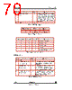
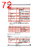
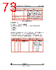
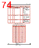
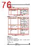
72 / 105 page  VV5410 & VV6410 Serial Control Bus cd5410-6410f-3-0.fm Commercial in confidence 72/105 [23], [17] - op_format Note: oeb_composite is the logical OR of op_format[5] and the OEB pin. [24], [18] - mode_select This register allows the user to configure the sensor to operate with the present generation of coprocessors as well as anticipated future devices. Bit Function Default Comment 1:0 Data format select. 0 00 - 5 wire parallel output 01 - 4 wire parallel output 1x - 8 wire parallel output Note: If the 8 wire output option has been selected then the FST and LST pins will output data bits 5 and 6 respectively, normal FST and LST function is not available 2 Embedded SAV/EAV Escape Sequences1 On / Off 1. Please note that if the embedded coding sequences are disabled then the FST signal is also disabled. The QCK output will continue to function IF the free running option has been selected. The LST functionality is unaffected by the state of this bit. 0 0 - Insert Embedded Control Sequences e.g Start and End of Active Video into Output Video data 1 - Pass-through mode. Output Video data equals ADC data. 4:3 reserved 11 5 Tri-state output data bus Enabled / Tri-state 0 On power up the data bus pads are enabled by default. This bit is OR’ed with the OEB pin to generate the enable signal for the data pins as detailed in Table 44 6 Re-time tri-state update. Off / On 0 Re-time new tri-state value to a field boundary. This bit affects the updating of the op_format[5] as well as data_format[6:5] 7 unused 0 Table 43 : [23], [17] - op_format OEB pin op_format[5] oeb_composite Comments 0 0 0 Data outputs enabled. 0 1 1 Data outputs are tri-stated by op_format[5] 1 0 1 Data outputs are tri-stated by OEB pin. 1 1 1 Data outputs are tri-stated. Table 44 : Data bus output control Bit Function Default Comment 0 Coprocessor device is VP3 No/Yes 1 By default the sensor expects the coprocessor to be a VP3 device. If the sensor is not being used with a VP3 device then this bit should be reset. This bit controls the arrangement of black/dark/visible lines within the field. It does not alter timing. Please see Table 45 : [24], [18] - Mode Select |
|
链接网址 |
| ALLDATASHEET是否为您带来帮助? [ DONATE ] |
关于 Alldatasheet | 广告服务 | 联系我们 | 隐私政策 | 数据表链接 | 链接交换 | 制造商名单 All Rights Reserved©Alldatasheet.com |
| Russian : Alldatasheetru.com | Korean : Alldatasheet.co.kr | Spanish : Alldatasheet.es | French : Alldatasheet.fr | Italian : Alldatasheetit.com Portuguese : Alldatasheetpt.com | Polish : Alldatasheet.pl | Vietnamese : Alldatasheet.vn Indian : Alldatasheet.in | Mexican : Alldatasheet.com.mx | British : Alldatasheet.co.uk | New Zealand : Alldatasheet.co.nz |
|
Family Site : ic2ic.com |
icmetro.com |
 Chinese ▼
 English
 Chinese
 German
 Japanese
 Russian
 Korean
 Spanish
 French
 Italian
 Portuguese
 Polish
 Vietnamese
 Indian
 Mexican
 British
 New Zealand