|
数据搜索系统,热门电子元器件搜索 |
|
|
数据搜索系统,热门电子元器件搜索 |
|
AD8551ARM-R2 数据表(PDF) 19 Page - Analog Devices |
|
|
|||||||||||||||||||||||||||||
AD8551ARM-R2 数据表(HTML) 19 Page - Analog Devices |
|
|
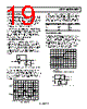
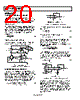
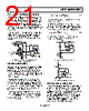
19 / 24 page  AD8551/AD8552/AD8554 Rev. C | Page 19 of 24 OUTPUT PHASE REVERSAL Output phase reversal occurs in some amplifiers when the input common-mode voltage range is exceeded. As common-mode voltage moves outside of the common-mode range, the outputs of these amplifiers suddenly jump in the opposite direction to the supply rail. This is the result of the differential input pair shutting down and causing a radical shifting of internal voltages, resulting in the erratic output behavior. The AD855x amplifiers have been carefully designed to prevent any output phase reversal, provided both inputs are maintained within the supply voltages. If there is the potential of one or both inputs exceeding either supply voltage, place a resistor in series with the input to limit the current to less than 2 mA to ensure the output does not reverse its phase. CAPACITIVE LOAD DRIVE The AD855x family has excellent capacitive load driving capabilities and can safely drive up to 10 nF from a single 5 V supply. Although the device is stable, capacitive loading limits the bandwidth of the amplifier. Capacitive loads also increase the amount of overshoot and ringing at the output. An R-C snubber network, shown in Figure 61, can be used to compensate the amplifier against capacitive load ringing and overshoot. 5V VIN 200mV p-p RX 60Ω CX 0.47µF CL 4.7nF VOUT AD8551/ AD8552/ AD8554 Figure 61. Snubber Network Configuration for Driving Capacitive Loads Although the snubber does not recover the loss of amplifier bandwidth from the load capacitance, it does allow the amplifier to drive larger values of capacitance while maintaining a minimum of overshoot and ringing. Figure 62 shows the output of an AD855x driving a 1 nF capacitor with and without a snubber network. WITH SNUBBER WITHOUT SNUBBER 10µs 100mV VSY = 5V CLOAD = 4.7nF Figure 62. Overshoot and Ringing are Substantially Reduced Using a Snubber Network The optimum value for the resistor and capacitor is a function of the load capacitance and is best determined empirically because actual CLOAD (CL) includes stray capacitances and may differ substantially from the nominal capacitive load. Table 5 shows some snubber network values that can be used as starting points. Table 5. Snubber Network Values for Driving Capacitive Loads CLOAD RX CX 1 nF 200 Ω 1 nF 4.7 nF 60 Ω 0.47 μF 10 nF 20 Ω 10 μF POWER-UP BEHAVIOR At power-up, the AD855x settles to a valid output within 5 μs. Figure 63 shows an oscilloscope photo of the output of the amplifier with the power supply voltage, and Figure 64 shows the test circuit. With the amplifier configured for unity gain, the device takes approximately 5 μs to settle to its final output voltage. This turn-on response time is much faster than most other autocorrection amplifiers, which can take hundreds of microseconds or longer for their output to settle. V+ 0V 0V VOUT 5µs 1V BOTTOM TRACE = 2V/DIV TOP TRACE = 1V/DIV Figure 63. AD855x Output Behavior on Power-Up VOUT AD8551/ AD8552/ AD8554 VSY = 0V TO 5V 100kΩ 100kΩ Figure 64. AD855x Test Circuit for Turn-On Time |
|
|
链接网址 |
| ALLDATASHEET是否为您带来帮助? [ DONATE ] |
关于 Alldatasheet | 广告服务 | 联系我们 | 隐私政策 | 数据表链接 | 链接交换 | 制造商名单 All Rights Reserved©Alldatasheet.com |
| Russian : Alldatasheetru.com | Korean : Alldatasheet.co.kr | Spanish : Alldatasheet.es | French : Alldatasheet.fr | Italian : Alldatasheetit.com Portuguese : Alldatasheetpt.com | Polish : Alldatasheet.pl | Vietnamese : Alldatasheet.vn Indian : Alldatasheet.in | Mexican : Alldatasheet.com.mx | British : Alldatasheet.co.uk | New Zealand : Alldatasheet.co.nz |
|
Family Site : ic2ic.com |
icmetro.com |
 Chinese ▼
 English
 Chinese
 German
 Japanese
 Russian
 Korean
 Spanish
 French
 Italian
 Portuguese
 Polish
 Vietnamese
 Indian
 Mexican
 British
 New Zealand