|
数据搜索系统,热门电子元器件搜索 |
|
|
数据搜索系统,热门电子元器件搜索 |
|
AD8055ART-R2 数据表(PDF) 13 Page - Analog Devices |
|
|
|||||||||||||||||||||||||||||
AD8055ART-R2 数据表(HTML) 13 Page - Analog Devices |
|
|
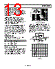
13 / 16 page  AD8055/AD8056 Rev. J | Page 13 of 16 FREQUENCY (MHz) 5 4 –5 1 –2 –3 –4 3 2 –1 0 0.3 1 10 100 500 CL 402Ω 100Ω 402Ω 50Ω VIN =0dBm CL =0pF CL = 10pF CL = 20pF CL =30pF POWER DISSIPATION LIMITS With a 10 V supply (total VCC − VEE), the quiescent power dissipation of the AD8055 in the SOT-23-5 package is 65 mW, while the quiescent power dissipation of the AD8056 in the MSOP-8 is 120 mW. This translates into a 15.6°C rise above the ambient for the SOT-23-5 package and a 24°C rise for the MSOP-8 package. The power dissipated under heavy load conditions is approximately equal to the supply voltage minus the output voltage, times the load current, plus the quiescent power previously computed. The total power dissipation is then multiplied by the thermal resistance of the package to find the temperature rise, above ambient, of the part. The junction temperature should be kept below 150°C. Figure 39. Capacitive Load Drive In general, to minimize peaking or to ensure the stability for larger values of capacitive loads, a small series resistor, R The AD8055 in the SOT-23-5 package can dissipate 270 mW, while the AD8056 in the MSOP-8 package can dissipate 325 mW (at 85°C ambient) without exceeding the maximum die temperature. In the case of the AD8056, this is greater than 1.5 V rms into 50 Ω, enough to accommodate a 4 V p-p sine wave signal on both outputs simultaneously. However, because each output of the AD8055 or AD8056 is capable of supplying as much as 110 mA into a short circuit, a continuous short- circuit condition will exceed the maximum safe junction temperature. S , can be added between the op amp output and the capacitor, CL. For the setup depicted in Figure 40, the relationship between RS and C RESISTOR SELECTION Table 3 is a guide for resistor selection for maintaining gain flatness vs. frequency for various values of gain. Table 3. Gain RF (Ω) RG (Ω) −3 dB Bandwidth (MHz) +1 0 300 +2 402 402 160 +5 1 k 249 45 +10 909 100 20 DRIVING CAPACITIVE LOADS When driving a capacitive load, most op amps exhibit peaking in the frequency response just before the frequency rolls off. Figure 39 shows the responses for an AD8056 running at a gain of +2, with an 100 Ω load that is shunted by various values of capacitance. It can be seen that under these conditions the part is still stable with capacitive loads of up to 30 pF. L was empirically derived and is shown in Figure 41. RS was chosen to produce less than 1 dB of peaking in the frequency response. Note also that after a sharp rise, RS quickly settles to approximately 25 Ω. 50Ω AD8055 +5V –5V 402Ω 402Ω 6 7 2 3 4 FET PROBE VIN =0dBm VOUT RS CL 0.1µF 10µF 0.1µF 10µF Figure 40. Setup for R vs. C S L 40 0 35 20 15 10 5 30 25 CL (pF) 0 1020 3040 5060 270 Figure 41. R vs. C S L |
|
|
链接网址 |
| ALLDATASHEET是否为您带来帮助? [ DONATE ] |
关于 Alldatasheet | 广告服务 | 联系我们 | 隐私政策 | 数据表链接 | 链接交换 | 制造商名单 All Rights Reserved©Alldatasheet.com |
| Russian : Alldatasheetru.com | Korean : Alldatasheet.co.kr | Spanish : Alldatasheet.es | French : Alldatasheet.fr | Italian : Alldatasheetit.com Portuguese : Alldatasheetpt.com | Polish : Alldatasheet.pl | Vietnamese : Alldatasheet.vn Indian : Alldatasheet.in | Mexican : Alldatasheet.com.mx | British : Alldatasheet.co.uk | New Zealand : Alldatasheet.co.nz |
|
Family Site : ic2ic.com |
icmetro.com |
 Chinese ▼
 English
 Chinese
 German
 Japanese
 Russian
 Korean
 Spanish
 French
 Italian
 Portuguese
 Polish
 Vietnamese
 Indian
 Mexican
 British
 New Zealand