|
数据搜索系统,热门电子元器件搜索 |
|
|
数据搜索系统,热门电子元器件搜索 |
|
AD8337BCPZ-R2 数据表(PDF) 22 Page - Analog Devices |
|
|
|||||||||||||||||||||||||||||
AD8337BCPZ-R2 数据表(HTML) 22 Page - Analog Devices |
|
|
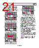
22 / 24 page  AD8337 Rev. B | Page 22 of 24 The offset voltage effect of the AD8337, as with all VGAs, can appear as a complex waveform when observed across the range of VGAIN voltage. Generated by multiple sources, each device has a unique VOS profile while the GAIN input is swept through its voltage range. The offset voltage profile seen in Figure 15 is a typical example. If the VGAIN input voltage is modulated, the output is the product of the VGAIN and the dc profile of the offset voltage, and it can be observed on a scope as a small ac signal as shown in Figure 74. In Figure 74, the signal applied to the VGAIN input is a 1 kHz ramp, and the output voltage signal is slightly less than 4 mV p-p. Under certain circumstances, the product of VGAIN and the offset profile plus spikes is a coherent spurious signal within the signal band of interest and indistinguishable from desired signals. In general, the slower the ramp applied to the GAIN pin, the smaller the spikes are. In most applications, these effects are benign and not an issue. THERMAL CONSIDERATIONS The thermal performance of LFCSPs, such as the AD8337, departs significantly from that of leaded devices such as the larger TSSOP or QFSP. In larger packages, heat is conducted away from the die by the path provided by the bond wires and the device leads. In LFCSPs, the heat transfer mechanisms are surface-to-air radiation from the top and side surfaces of the package and conduction through the metal solder pad on the mounting surface of the device. –4 6 10 0 4 8 –800 –2 VGAIN (mV) –600 –200 –400 400 600 200 800 0 2 –10 –8 –6 VS = 2.5 INPUT OUTPUT VS = ±2.5V θJC is the traditional thermal metric found in the data sheets of integrated circuits. Heat transfer away from the die is a 3- dimensional dynamic, and the path is through the bond wires, leads, and the six surfaces of the package. Because of the small size of LFCSPs, the θJC is not measured conventionally; instead, it is calculated using thermodynamic rules. The θJC value of the AD8837 listed in Table 2 assumes that the tab is soldered to the board and that there are three additional ground layers beneath the device connected by at least four vias. For a device with an unsoldered pad, the θJC nearly doubles, becoming 138°C/W. Figure 74. Offset Voltage vs. VGAIN for a 1 kHz Ramp The profile of the waveform shown in Figure 74 is consistent over a wide range of signals from dc to about 20 kHz. Above 20 kHz, secondary artifacts can be generated due to the effects of minor internal circuit tolerances, as seen in Figure 75. These artifacts are caused by settling and time constants of the inter- polator circuit and appear at the output as the voltage spikes seen in Figure 75. PSI (Ψ) Table 2 lists a subset of the classic theta specification, ΨJT (Psi junction to top). θJC is the metric of heat transfer from the die to the case, involving the six outside surfaces of the package. Ψ(XY) is a subset of the theta value and the thermal gradient from the junction (die) to each of the six surfaces. Ψ can be different for each of the surfaces, but since the top of the package is actually a fraction of a millimeter from the die, the surface temperature of the package is very close to the die temperature. The die temperature is calculated as the product of the power dissipation and ΨJT. Since the top surface tempera- ture and power dissipation are easily measured, it follows that the die temperature is easily calculated. For example, for a dissipation of 180 mW and a ΨJT of 5.3°C/W, the die temperature is slightly less than 1°C higher than the surface temperature. –4 6 10 0 4 8 –800 –2 VGAIN (mV) –600 –200 –400 400 600 200 800 0 2 –10 –8 –6 VS = 2.5 INPUT OUTPUT SPIKE SPIKE VS = ±2.5V BOARD LAYOUT Because the AD8337 is a high frequency device, board layout is critical. It is very important to have a good ground plane connection to the VCOM pin. Coupling through the ground plane, from the output to the input, can cause peaking at higher frequencies. Figure 75. VOS Profile for a 50 kHz Ramp |
|
|
链接网址 |
| ALLDATASHEET是否为您带来帮助? [ DONATE ] |
关于 Alldatasheet | 广告服务 | 联系我们 | 隐私政策 | 数据表链接 | 链接交换 | 制造商名单 All Rights Reserved©Alldatasheet.com |
| Russian : Alldatasheetru.com | Korean : Alldatasheet.co.kr | Spanish : Alldatasheet.es | French : Alldatasheet.fr | Italian : Alldatasheetit.com Portuguese : Alldatasheetpt.com | Polish : Alldatasheet.pl | Vietnamese : Alldatasheet.vn Indian : Alldatasheet.in | Mexican : Alldatasheet.com.mx | British : Alldatasheet.co.uk | New Zealand : Alldatasheet.co.nz |
|
Family Site : ic2ic.com |
icmetro.com |
 Chinese ▼
 English
 Chinese
 German
 Japanese
 Russian
 Korean
 Spanish
 French
 Italian
 Portuguese
 Polish
 Vietnamese
 Indian
 Mexican
 British
 New Zealand