6-29
RF2638
Rev B15 060921
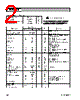
Pin
Function
Description
Interface Schematic
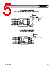
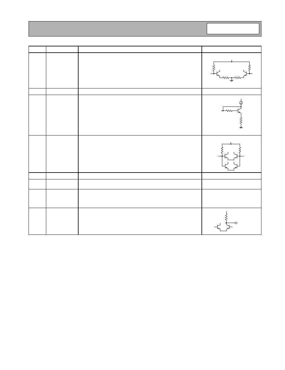
1IF-
Balanced IF input pin. This pin is internally DC-biased and should be
DC-blocked if connected to a device with a DC level present. For single-
ended input operation, one pin is used as an input and the other IF
input is AC-coupled to ground. The balanced, input impedance is
260
Ω.
2IF+
Same as pin 1, except complementary input.
See pin 1.
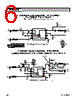
3BYP
Bypass pin for internal bias circuitry. Bypass with a 1nF capacitor.
4LO-
Balanced LO input pin. This pin is internally DC-biased and should be
DC-blocked if connected to a device with a DC level present. For single-
ended input operation, one pin is used as an input and the other LO
input is AC-coupled to ground.
5LO+
Same as pin 4, except complementary input.
See pin 4.
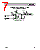
6GND
Ground connection. For best performance, keep traces physically short
and connect immediately to ground plane.
7VCC
Supply voltage pin. External bypassing is required. External RF, LO,
and IF bypassing is required. The trace length between the pin and the
bypass capacitors should be minimized. The ground side of the bypass
capacitors should connect immediately to ground plane.
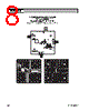
8RF OUT
RF output pin.
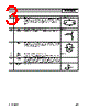
IF+
IF-
130
Ω
130
Ω
BIAS
BYP
LO+
LO-
BIAS
300
Ω
RF OUT

 Chinese ▼
 English
 Chinese
 German
 Japanese
 Russian
 Korean
 Spanish
 French
 Italian
 Portuguese
 Polish
 Vietnamese
 Indian
 Mexican
 British
 New Zealand