|
数据搜索系统,热门电子元器件搜索 |
|
|
数据搜索系统,热门电子元器件搜索 |
|
LTC2913CMS-2 数据表(PDF) 5 Page - Linear Technology |
|
|
|||||||||||||||||||||||||||||
LTC2913CMS-2 数据表(HTML) 5 Page - Linear Technology |
|
|
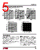
5 / 12 page  LTC2913 5 2913fa UV Output Voltage vs VCC UV, ISINK vs VCC PIN FUNCTIONS UV/OV Voltage Output Low vs Output Sink Current TYPICAL PERFORMANCE CHARACTERISTICS Reset Timeout Period vs Temperature Reset Timeout Period vs Capacitance DIS (Pin 8, LTC2913-2): Output Disable Input. Disables the OV and UV output pins. When DIS is pulled high, the OV and UV pins are not asserted except during a UVLO condition. DIS has a weak (2µA) internal pull-down to GND. Leave DIS open if unused. Exposed Pad (Pin 11, DFN Package): Exposed Pad may be left open or connected to device ground. GND (Pin 5): Device Ground. LATCH (Pin 8, LTC2913-1): OV Latch Clear/Bypass Input. When pin is pulled low, OV is latched when asserted. When pulled high, OV latch is cleared. While held high, OV has the same delay and output characteristics as UV. OV (Pin 6): Overvoltage Logic Output. Asserts low when either VL input voltage is above threshold. Latched low (LTC2913-1). Held low for programmed delay time after both VL inputs are valid (LTC2913-2). OV has a weak pull- up to VCC and may be pulled above VCC using an external pull-up. Leave OV open if unused. SUPPLY VOLTAGE, VCC (V) 0 3 4 5 4 2913 G07 2 1 0 1 2 3 5 VHn = 0.55V SEL = VCC SUPPLY VOLTAGE, VCC (V) 0 3 4 5 4 2913 G08 2 1 0 1 2 3 5 UV AT 150mV UV AT 50mV VHn = 0.45V SEL = VCC IUV/OV (mA) 0 0 0.2 0.4 0.6 0.8 1.0 125 °C –40 °C 25 °C 5 10 15 20 2913 G09 25 30 TEMPERATURE ( °C) –50 6 7 8 9 10 12 –25 0 25 50 2913 G10 75 100 11 CTMR = 1nF TMR PIN CAPACITANCE, CTMR (nF) 0.1 1 1 100 10000 10 100 1000 2913 G11 10 1000 Specifications are at TA = 25°C, VCC = 3.3V unless otherwise noted. |
|
|
链接网址 |
| ALLDATASHEET是否为您带来帮助? [ DONATE ] |
关于 Alldatasheet | 广告服务 | 联系我们 | 隐私政策 | 数据表链接 | 链接交换 | 制造商名单 All Rights Reserved©Alldatasheet.com |
| Russian : Alldatasheetru.com | Korean : Alldatasheet.co.kr | Spanish : Alldatasheet.es | French : Alldatasheet.fr | Italian : Alldatasheetit.com Portuguese : Alldatasheetpt.com | Polish : Alldatasheet.pl | Vietnamese : Alldatasheet.vn Indian : Alldatasheet.in | Mexican : Alldatasheet.com.mx | British : Alldatasheet.co.uk | New Zealand : Alldatasheet.co.nz |
|
Family Site : ic2ic.com |
icmetro.com |
 Chinese ▼
 English
 Chinese
 German
 Japanese
 Russian
 Korean
 Spanish
 French
 Italian
 Portuguese
 Polish
 Vietnamese
 Indian
 Mexican
 British
 New Zealand