|
数据搜索系统,热门电子元器件搜索 |
|
|
数据搜索系统,热门电子元器件搜索 |
|
AD637JRZ-R7 数据表(PDF) 21 Page - Analog Devices |
|
|
|||||||||||||||||||||||||||||
AD637JRZ-R7 数据表(HTML) 21 Page - Analog Devices |
|
|
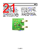
21 / 25 page  Data Sheet AD637 Rev. L | Page 21 of 25 EVALUATION BOARD Figure 23 shows a digital image of the AD637-EVALZ, an evaluation board specially designed for the AD637. It is available at www.analog.com and is fully tested and ready for bench testing after connecting power and signal I/O. The circuit is configured for dual power supplies, and standard BNC connectors serve as the signal input and output ports. Referring to the schematic in Figure 30, the input connector RMS_IN is capacitively coupled to Pin 15 (VIN of SOIC package) of the AD637. The DC_OUT connector is connected to Pin 11, RMS OUT, with provisions for connections to the output buffer between Pin 1 and Pin 16. The buffer is an uncommitted op amp, and is configured on the AD637-EVALZ as a low-pass Sallen-Key filter whose fC < 0.5 Hz. Users can connect to the buffer by moving the FILTER switch to the on position. DC_OUT is still the output of the AD637, and the test loop, BUF_OUT, is the output of the buffer. The R2 trimmer adjusts the output offset voltage. The LPF frequency is changed by changing the component values of CF1, CF2, R4, and R5. See Figure 24 and Figure 30 to locate these components. Note that a wide range of capacitor and resistor values can be used with the AD637 buffer amplifier. Figure 23. AD637-EVALZ |
|
|
链接网址 |
| ALLDATASHEET是否为您带来帮助? [ DONATE ] |
关于 Alldatasheet | 广告服务 | 联系我们 | 隐私政策 | 数据表链接 | 链接交换 | 制造商名单 All Rights Reserved©Alldatasheet.com |
| Russian : Alldatasheetru.com | Korean : Alldatasheet.co.kr | Spanish : Alldatasheet.es | French : Alldatasheet.fr | Italian : Alldatasheetit.com Portuguese : Alldatasheetpt.com | Polish : Alldatasheet.pl | Vietnamese : Alldatasheet.vn Indian : Alldatasheet.in | Mexican : Alldatasheet.com.mx | British : Alldatasheet.co.uk | New Zealand : Alldatasheet.co.nz |
|
Family Site : ic2ic.com |
icmetro.com |
 Chinese ▼
 English
 Chinese
 German
 Japanese
 Russian
 Korean
 Spanish
 French
 Italian
 Portuguese
 Polish
 Vietnamese
 Indian
 Mexican
 British
 New Zealand