|
数据搜索系统,热门电子元器件搜索 |
|
|
数据搜索系统,热门电子元器件搜索 |
|
TC1027CEPR 数据表(PDF) 6 Page - Microchip Technology |
|
|
|||||||||||||||||||||||||||||
TC1027CEPR 数据表(HTML) 6 Page - Microchip Technology |
|
|
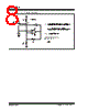
6 / 18 page  TC1027 DS21284B-page 6 © 2002 Microchip Technology Inc. Capacitor C1 will charge up through R4. When the voltage at the comparator’s inverting input is equal to VH, the comparator output will switch. With the output at ground potential, the value at the non-inverting input terminal (VL) is reduced by the hysteresis network to a value given by: EQUATION 4-7: Using the same resistors as before, capacitor C1 must now discharge through R4 toward ground. The output will return to a high state when the voltage across the capacitor has discharged to a value equal to VL.The period of oscillation will be twice the time it takes for the RC circuit to charge up to one half its final value. The period can be calculated from: EQUATION 4-8: The frequency stability of this circuit should only be a function of the external component tolerances. Figure 4-6 shows the circuit for a pulse width modulator circuit. It is essentially the same as in Figure 4-4, but with the addition of an input control voltage. When the input control voltage is equal to one-half VDD, operation is basically the same as described for the free-running oscillator. If the input control voltage is moved above or below one-half VDD, the duty cycle of the output square wave will be altered. This is because the addition of the control voltage at the input has now altered the trip points. The equations for these trip points are shown in Figure 4-6 (see VH and VL). Pulse width sensitivity to the input voltage variations can be increased by reducing the value of R6 from 10k Ω and conversely, sensitivity will be reduced by increasing the value of R6. The values of R1 and C1 can be varied to produce the desired center frequency. FIGURE 4-1: COMPARATOR EXTERNAL HYSTERESIS CONFIGURATION FIGURE 4-2: PRECISION BATTERY MONITOR V L V DD 3 ----------- = 1 FREQ ----------------- 2 0.694 () R4 () C1 () = + – VR VDD VOUT VSRC RA RB RC 1/4 TC1027 VDD VDD VDD R2, 330k, 1% TC1034 1/4 R4, 470k, 1% R5, 7.5M 1/4 R6, 7.5M R3, 470k, 1% R1, 270k, 1% VR To System DC/DC Converter 3V Alkaline TC1027 BATTFAIL BATTLOW CMPTR1 + – CMPTR2 + – AMP1 + – + |
|
|
链接网址 |
| ALLDATASHEET是否为您带来帮助? [ DONATE ] |
关于 Alldatasheet | 广告服务 | 联系我们 | 隐私政策 | 数据表链接 | 链接交换 | 制造商名单 All Rights Reserved©Alldatasheet.com |
| Russian : Alldatasheetru.com | Korean : Alldatasheet.co.kr | Spanish : Alldatasheet.es | French : Alldatasheet.fr | Italian : Alldatasheetit.com Portuguese : Alldatasheetpt.com | Polish : Alldatasheet.pl | Vietnamese : Alldatasheet.vn Indian : Alldatasheet.in | Mexican : Alldatasheet.com.mx | British : Alldatasheet.co.uk | New Zealand : Alldatasheet.co.nz |
|
Family Site : ic2ic.com |
icmetro.com |
 Chinese ▼
 English
 Chinese
 German
 Japanese
 Russian
 Korean
 Spanish
 French
 Italian
 Portuguese
 Polish
 Vietnamese
 Indian
 Mexican
 British
 New Zealand