|
数据搜索系统,热门电子元器件搜索 |
|
|
数据搜索系统,热门电子元器件搜索 |
|
AD8031ART-R2 数据表(PDF) 14 Page - Analog Devices |
|
|
|||||||||||||||||||||||||||||
AD8031ART-R2 数据表(HTML) 14 Page - Analog Devices |
|
|
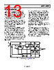
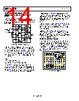
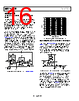
14 / 20 page  AD8031/AD8032 Data Sheet Rev. G | Page 14 of 20 OUTPUT STAGE, OPEN-LOOP GAIN AND DISTORTION vs. CLEARANCE FROM POWER SUPPLY The AD8031 features a rail-to-rail output stage. The output transistors operate as common-emitter amplifiers, providing the output drive current as well as a large portion of the amplifier’s open-loop gain. DIFFERENTIAL DRIVE FROM INPUT STAGE Q37 Q47 Q21 Q20 Q51 Q27 Q68 Q44 Q42 Q48 Q49 Q50 Q43 VOUT Q38 I1 25µA I2 25µA C9 5pF C5 1.5pF I5 25µA I4 25µA R29 300 Ω Figure 44. Output Stage Simplified Schematic The output voltage limit depends on how much current the output transistors are required to source or sink. For applications with low drive requirements (for instance, a unity gain follower driving another amplifier input), the AD8031 typically swings within 20 mV of either voltage supply. As the required current load increases, the saturation output voltage increases linearly as ILOAD × RC where: ILOAD is the required load current. RC is the output transistor collector resistance. For the AD8031, the collector resistances for both output transistors are typically 25 Ω. As the current load exceeds the rated output current of 15 mA, the amount of base drive current required to drive the output transistor into saturation reaches its limit, and the amplifier’s output swing rapidly decreases. The open-loop gain of the AD8031 decreases approximately linearly with load resistance and depends on the output voltage. Open-loop gain stays constant to within 250 mV of the positive power supply, 150 mV of the negative power supply, and then decreases as the output transistors are driven further into saturation. The distortion performance of the AD8031/AD8032 amplifiers differs from conventional amplifiers. Typically, the distortion performance of the amplifier degrades as the output voltage amplitude increases. Used as a unity gain follower, the output of the AD8031/ AD8032 exhibits more distortion in the peak output voltage region around VCC − 0.7 V. This unusual distortion characteristic is caused by the input stage architecture and is discussed in detail in the Input Stage Operation section, OUTPUT OVERDRIVE RECOVERY Output overdrive of an amplifier occurs when the amplifier attempts to drive the output voltage to a level outside its normal range. After the overdrive condition is removed, the amplifier must recover to normal operation in a reasonable amount of time. As shown in Figure 45, the AD8031/AD8032 recover within 100 ns from negative overdrive and within 80 ns from positive overdrive. RL 50 Ω VIN VOUT 100ns 1V VS = ±2.5V VIN = ±2.5V RL = 1kΩ TO GND RF = RG = 2kΩ RG RF Figure 45. Overdrive Recovery |
|
|
链接网址 |
| ALLDATASHEET是否为您带来帮助? [ DONATE ] |
关于 Alldatasheet | 广告服务 | 联系我们 | 隐私政策 | 数据表链接 | 链接交换 | 制造商名单 All Rights Reserved©Alldatasheet.com |
| Russian : Alldatasheetru.com | Korean : Alldatasheet.co.kr | Spanish : Alldatasheet.es | French : Alldatasheet.fr | Italian : Alldatasheetit.com Portuguese : Alldatasheetpt.com | Polish : Alldatasheet.pl | Vietnamese : Alldatasheet.vn Indian : Alldatasheet.in | Mexican : Alldatasheet.com.mx | British : Alldatasheet.co.uk | New Zealand : Alldatasheet.co.nz |
|
Family Site : ic2ic.com |
icmetro.com |
 Chinese ▼
 English
 Chinese
 German
 Japanese
 Russian
 Korean
 Spanish
 French
 Italian
 Portuguese
 Polish
 Vietnamese
 Indian
 Mexican
 British
 New Zealand