|
数据搜索系统,热门电子元器件搜索 |
|
|
数据搜索系统,热门电子元器件搜索 |
|
AD8067ARTZ-R2 数据表(PDF) 15 Page - Analog Devices |
|
|
|||||||||||||||||||||||||||||
AD8067ARTZ-R2 数据表(HTML) 15 Page - Analog Devices |
|
|
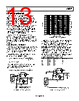
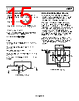
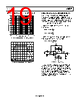
15 / 24 page  Data Sheet AD8067 Rev. B | Page 15 of 24 DC ERROR CALCULATIONS Figure 44 illustrates the primary dc errors associated with a voltage feedback amplifier. For both inverting and noninverting configurations: + = G F G OS OS R R R V V to due Error Voltage Output F B– G G F S B B R I R R R R I I to due Error Voltage Output × + × = + – Total error is the sum of the two. DC common-mode and power supply effects can be added by modeling the total VOS with the expression: CMR V PSR V nom V tot V CM S OS OS Δ Δ ) ( ) ( + + = where: VOS (nom) is the offset voltage specified at nominal conditions (1 mV max). ∆VS is the change in power supply voltage from nominal conditions. PSR is power supply rejection (90 dB minimum). ∆VCM is the change in common-mode voltage from nominal test conditions. CMR is the common-mode rejection (85 dB minimum for the AD8067). VI RS RG IB+ IB– – + VOUT – + – + +VOS– RF Figure 44. Op Amp DC Error Sources INPUT AND OUTPUT OVERLOAD BEHAVIOR A simplified schematic of the AD8067 input stage is shown in Figure 45. This shows the cascoded N-channel JFET input pair, the ESD and other protection diodes, and the auxiliary NPN input stage that eliminates phase inversion behavior. When the common-mode input voltage to the amplifier is driven to within approximately 3 V of the positive power supply, the input JFET’s bias current turns off, and the bias of the NPN pair turns on, taking over control of the amplifier. The NPN differential pair now sets the amplifier’s offset, and the input bias current is now in the range of several tens of microamps. This behavior is illustrated in Figure 25 and Figure 26. Normal operation resumes when the common-mode voltage goes below the 3 V from the positive supply threshold. The output transistors have circuitry included to limit the extent of their saturation when the output is overdriven. This improves output recovery time. A plot of the output recovery time for the AD8067 used as a G = +10 buffer is shown in Figure 17. VBIAS VCC VEE VEE VCC VP VN SWITCH CONTROL VEE VCC TO REST OF AMP VTHRESHOLD Figure 45. Simplified Input Schematic |
|
|
链接网址 |
| ALLDATASHEET是否为您带来帮助? [ DONATE ] |
关于 Alldatasheet | 广告服务 | 联系我们 | 隐私政策 | 数据表链接 | 链接交换 | 制造商名单 All Rights Reserved©Alldatasheet.com |
| Russian : Alldatasheetru.com | Korean : Alldatasheet.co.kr | Spanish : Alldatasheet.es | French : Alldatasheet.fr | Italian : Alldatasheetit.com Portuguese : Alldatasheetpt.com | Polish : Alldatasheet.pl | Vietnamese : Alldatasheet.vn Indian : Alldatasheet.in | Mexican : Alldatasheet.com.mx | British : Alldatasheet.co.uk | New Zealand : Alldatasheet.co.nz |
|
Family Site : ic2ic.com |
icmetro.com |
 Chinese ▼
 English
 Chinese
 German
 Japanese
 Russian
 Korean
 Spanish
 French
 Italian
 Portuguese
 Polish
 Vietnamese
 Indian
 Mexican
 British
 New Zealand