|
数据搜索系统,热门电子元器件搜索 |
|
|
数据搜索系统,热门电子元器件搜索 |
|
AD8045ACPZ-R2 数据表(PDF) 19 Page - Analog Devices |
|
|
|||||||||||||||||||||||||||||
AD8045ACPZ-R2 数据表(HTML) 19 Page - Analog Devices |
|
|
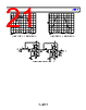
19 / 24 page  Data Sheet AD8045 Rev. C | Page 19 of 24 APPLICATIONS INFORMATION LOW DISTORTION PINOUT The AD8045 LFCSP features an Analog Devices new low distortion pinout. The new pinout provides two advantages over the traditional pinout. First, improved second harmonic distortion performance, which is accomplished by the physical separation of the noninverting input pin and the negative power supply pin. Second, the simplification of the layout due to the dedicated feedback pin and easy routing of the gain set resistor back to the inverting input pin. This allows a compact layout, which helps to minimize parasitics and increase stability. The traditional SOIC pinout has been slightly modified as well to incorporate a dedicated feedback pin. Pin 1, previously a no connect pin on the amplifier, is now a dedicated feedback pin. The new pinout reduces parasitics and simplifies the board layout. Existing applications that use the traditional SOIC pinout can take full advantage of the outstanding performance offered by the AD8045. An electrical insulator may be required if the SOIC rests on the ground plane or other metal trace. This is covered in more detail in the Exposed Paddle section of this data sheet. In existing designs, which have Pin 1 tied to ground or to another potential, simply lift Pin 1 of the AD8045 or remove the potential on the Pin 1 solder pad. The designer does not need to use the dedicated feedback pin to provide feedback for the AD8045. The output pin of the AD8045 can still be used to provide feedback to the inverting input of the AD8045. HIGH SPEED ADC DRIVER When used as an ADC driver, the AD8045 offers results comparable to transformers in distortion performance. Many ADC applications require that the analog input signal be dc-coupled and operate over a wide frequency range. Under these requirements, operational amplifiers are very effective interfaces to ADCs. An op amp interface provides the ability to amplify and level shift the input signal to be compatible with the input range of the ADC. Unlike transformers, operational amplifiers can be operated over a wide frequency range down to and including dc. Figure 67 shows the AD8045 as a dc-coupled differential driver for the AD9244, a 14-bit 65 MSPS ADC. The two amplifiers are configured in noninverting and inverting modes. Both amplifiers are set with a noise gain of +2 to provide better bandwidth matching. The inverting amplifier is set for a gain of –1, while the noninverting is set for a gain of +2. The noninverting input is divided by 2 in order to normalize its output and make it equal to the inverting output. This dc-coupled differential driver is best suited for ±5 V operation in which optimum distortion performance is required and the input signal is ground referenced. VINA VINB CML AD9244 511 Ω 511 Ω 511 Ω 511 Ω 511 Ω 511 Ω VIN VCML – VIN AD8045 AD8045 0.1 µF 20pF 1 µF 0.1 µF OP27 511 Ω 511 Ω VCML + VIN 33 Ω 33 Ω 2.5k Ω 100 Ω Figure 67. High Speed ADC Driver The outputs of the AD8045 devices are centered about the 2.5 V common-mode range of the AD9244. The common-mode reference voltage from the AD9244 is buffered and filtered via the OP27 and fed to the noninverting resistor network used in the level shifting circuit. The spurious-free dynamic range (SFDR) performance is shown in Figure 68. Figure 69 shows a 50 MHz single-tone FFT performance. INPUT FREQUENCY (MHz) 100 1 10 120 100 80 60 40 20 0 AD8045 Figure 68. SFDR vs. Frequency |
|
|
链接网址 |
| ALLDATASHEET是否为您带来帮助? [ DONATE ] |
关于 Alldatasheet | 广告服务 | 联系我们 | 隐私政策 | 数据表链接 | 链接交换 | 制造商名单 All Rights Reserved©Alldatasheet.com |
| Russian : Alldatasheetru.com | Korean : Alldatasheet.co.kr | Spanish : Alldatasheet.es | French : Alldatasheet.fr | Italian : Alldatasheetit.com Portuguese : Alldatasheetpt.com | Polish : Alldatasheet.pl | Vietnamese : Alldatasheet.vn Indian : Alldatasheet.in | Mexican : Alldatasheet.com.mx | British : Alldatasheet.co.uk | New Zealand : Alldatasheet.co.nz |
|
Family Site : ic2ic.com |
icmetro.com |
 Chinese ▼
 English
 Chinese
 German
 Japanese
 Russian
 Korean
 Spanish
 French
 Italian
 Portuguese
 Polish
 Vietnamese
 Indian
 Mexican
 British
 New Zealand