|
数据搜索系统,热门电子元器件搜索 |
|
|
数据搜索系统,热门电子元器件搜索 |
|
PT7C4050ADE 数据表(PDF) 3 Page - Pericom Semiconductor Corporation |
|
|
|||||||||||||||||||||||||||||
PT7C4050ADE 数据表(HTML) 3 Page - Pericom Semiconductor Corporation |
|
|
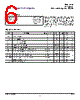
3 / 13 page  ||||||||||||||||||||||||||||||||||||||||||||||||||||||||||||||||||||||||||||||||||||||||||||||||||||||||||||||||||||||||||||||||||||||||||||||||||||||||||||||||||||||||||||||||||||||||||||||||||||||||||||||||||||||||||||||||||||||||||||||||||||||||||||||||||||||||||||||||||||||||||||||||||||||||||||||||||||||||||||||||||||||| PT0239L (06/07) Ver: 0 3 Data Sheet PT7C4050 PLL with Integrated VCXO Pin Description Pin Sym Description 1 X1 Crystal oscillator connected between X1 and X2 2 VC Control voltage input. It controls crystal oscillator (VCXO). 3 NC Not connected. 4 AGND Analog ground. 5 OPN Negative input. terminal to internal operational amplifier. 6 OPOUT Output. terminal of internal operational amplifier. 7 OPP Positive input. terminal to internal operational amplifier. 8 S1 9 S2 10 S3 S1, S2, S3 Options for selectable divider N 11 LOS-IN1 (LOSIN) TTL input. Internal pull down. Normally this pin is connected to OUT1 and selects REF-CLK1 input 12 PHO Output. signal produced by phase detector of data. 13 REF-CLK1 (DATAIN) Input clock signal. to phase detector (TTL switching thresholds for recovering DATAIN) 14 FB-CLK (CLKIN) TTL switching thresholds input. Connected to external feedback clock. 15 DGND Digital ground. 16 LOS Loss of signal detection. for DATAIN input. Refer to LOS detection description. 17 RCLK (CLK-OUT3) Output recovered clock. 18 RDATA (CLK-OUT4) Output recovered data stream. 19 DVDD Digital power supply. 20*1 CLK-OUT2 Output clock of internal VCXO frequency controlled by S3, S2, S1 while S4 set logic high 21 HIZ TTL input. When set to a logic low, output pins CLK-OUT1, CLK-OUT2, RCLK, and RDATA buffers are set to high-impedance state. When set to logic high or no connection, the device functions and output pins CLK-OUT1, CLK-OUT2, RCLK, and RDATA etc. are active. This input has an internal pull-up resistor. 22 CLK-OUT1 Output clock. of internal VCXO or half VCXO frequency, controlled by SEL-OUT1. 23*2 SEL-OUT1 CMOS input. ‘LO’ selects half of internal VCO frequency. ‘HI’ selects internal VCO frequency. Internal pull up. 24 GND Ground. 25 AVDD (XT-VDD) Analog power supply. 26 NC Not connected. 27 NC Not connected. 28 X2 Crystal oscillator connected between X1 and X2 Note: *1: S3, S2, S1 option for selectable divider N, Please refer to Table 1 *2: SEL-OUT1 option for VCXO or half VCXO output freq. Please refer to Table 2 ( ): For pin11/13/14/17/18/25, die option |
|
|
链接网址 |
| ALLDATASHEET是否为您带来帮助? [ DONATE ] |
关于 Alldatasheet | 广告服务 | 联系我们 | 隐私政策 | 数据表链接 | 链接交换 | 制造商名单 All Rights Reserved©Alldatasheet.com |
| Russian : Alldatasheetru.com | Korean : Alldatasheet.co.kr | Spanish : Alldatasheet.es | French : Alldatasheet.fr | Italian : Alldatasheetit.com Portuguese : Alldatasheetpt.com | Polish : Alldatasheet.pl | Vietnamese : Alldatasheet.vn Indian : Alldatasheet.in | Mexican : Alldatasheet.com.mx | British : Alldatasheet.co.uk | New Zealand : Alldatasheet.co.nz |
|
Family Site : ic2ic.com |
icmetro.com |
 Chinese ▼
 English
 Chinese
 German
 Japanese
 Russian
 Korean
 Spanish
 French
 Italian
 Portuguese
 Polish
 Vietnamese
 Indian
 Mexican
 British
 New Zealand