|
数据搜索系统,热门电子元器件搜索 |
|
|
数据搜索系统,热门电子元器件搜索 |
|
P4C1024L70CWC 数据表(PDF) 6 Page - Pyramid Semiconductor Corporation |
|
|
|||||||||||||||||||||||||||||
P4C1024L70CWC 数据表(HTML) 6 Page - Pyramid Semiconductor Corporation |
|
|
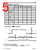
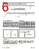
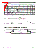
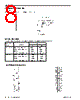
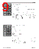
6 / 11 page  P4C1024L Page 6 of 10 Document # SRAM125 REV C D IN Write Active Read TIMING WAVEFORM OF WRITE CYCLE NO.2 (CE CE CE CE CE CONTROLLED)(6) * including scope and test fixture. Note: Because of the high speed of the P4C1024L, care must be taken when testing this device; an inadequate setup can cause a normal functioning part to be rejected as faulty. Long high-inductance leads that cause supply bounce must be avoided by bringing the V CC and ground planes directly up to the contactor fingers. A 0.01 µF high frequency capacitor is also required between V CC and ground. To avoid signal reflections, proper termination must be used; for example, a 50 Ω test environment should be terminated into a 50Ω load with 1.77V (Thevenin Voltage) at the comparator input, and a 589 Ω resistor must be used in series with D OUT to match 639Ω (Thevenin Resistance). AC TEST CONDITIONS TRUTH TABLE Input Pulse Levels Input Rise and Fall Times Input Timing Reference Level Output Timing Reference Level Output Load GND to 3.0V 3ns 1.5V 1.5V See Fig. 1 and 2 Mode Standby Standby D OUT Disabled Standby Power I/O WE WE WE WE WE OE OE OE OE OE CE 2 CE CE CE CE CE 1 High Z High Z D OUT X X H H L X X H L X X L H H H H X L L L Standby Active Active High Z Figure 1. Output Load Figure 2. Thevenin Equivalent |
|
|
链接网址 |
| ALLDATASHEET是否为您带来帮助? [ DONATE ] |
关于 Alldatasheet | 广告服务 | 联系我们 | 隐私政策 | 数据表链接 | 链接交换 | 制造商名单 All Rights Reserved©Alldatasheet.com |
| Russian : Alldatasheetru.com | Korean : Alldatasheet.co.kr | Spanish : Alldatasheet.es | French : Alldatasheet.fr | Italian : Alldatasheetit.com Portuguese : Alldatasheetpt.com | Polish : Alldatasheet.pl | Vietnamese : Alldatasheet.vn Indian : Alldatasheet.in | Mexican : Alldatasheet.com.mx | British : Alldatasheet.co.uk | New Zealand : Alldatasheet.co.nz |
|
Family Site : ic2ic.com |
icmetro.com |
 Chinese ▼
 English
 Chinese
 German
 Japanese
 Russian
 Korean
 Spanish
 French
 Italian
 Portuguese
 Polish
 Vietnamese
 Indian
 Mexican
 British
 New Zealand