|
数据搜索系统,热门电子元器件搜索 |
|
|
数据搜索系统,热门电子元器件搜索 |
|
M93C76-RBN3G/S 数据表(PDF) 18 Page - STMicroelectronics |
|
|
|||||||||||||||||||||||||||||
M93C76-RBN3G/S 数据表(HTML) 18 Page - STMicroelectronics |
|
|
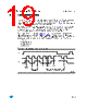
18 / 38 page  READY/BUSY status M93C86, M93C76, M93C66, M93C56, M93C46 18/38 6 READY/BUSY status While the Write or Erase cycle is underway, for a WRITE, ERASE, WRAL or ERAL instruction, the Busy signal (Q=0) is returned whenever Chip Select input (S) is driven high. (Please note, though, that there is an initial delay, of tSLSH, before this status information becomes available). In this state, the M93Cx6 ignores any data on the bus. When the Write cycle is completed, and Chip Select Input (S) is driven high, the Ready signal (Q=1) indicates that the M93Cx6 is ready to receive the next instruction. Serial Data Output (Q) remains set to 1 until the Chip Select Input (S) is brought low or until a new start bit is decoded. 7 Initial delivery state The device is delivered with all bits in the memory array set to 1 (each byte contains FFh). 8 Common I/O operation Serial Data Output (Q) and Serial Data Input (D) can be connected together, through a current limiting resistor, to form a common, single-wire data bus. Some precautions must be taken when operating the memory in this way, mostly to prevent a short circuit current from flowing when the last address bit (A0) clashes with the first data bit on Serial Data Output (Q). Please see the application note AN394 for details. |
|
链接网址 |
| ALLDATASHEET是否为您带来帮助? [ DONATE ] |
关于 Alldatasheet | 广告服务 | 联系我们 | 隐私政策 | 数据表链接 | 链接交换 | 制造商名单 All Rights Reserved©Alldatasheet.com |
| Russian : Alldatasheetru.com | Korean : Alldatasheet.co.kr | Spanish : Alldatasheet.es | French : Alldatasheet.fr | Italian : Alldatasheetit.com Portuguese : Alldatasheetpt.com | Polish : Alldatasheet.pl | Vietnamese : Alldatasheet.vn Indian : Alldatasheet.in | Mexican : Alldatasheet.com.mx | British : Alldatasheet.co.uk | New Zealand : Alldatasheet.co.nz |
|
Family Site : ic2ic.com |
icmetro.com |
 Chinese ▼
 English
 Chinese
 German
 Japanese
 Russian
 Korean
 Spanish
 French
 Italian
 Portuguese
 Polish
 Vietnamese
 Indian
 Mexican
 British
 New Zealand