|
数据搜索系统,热门电子元器件搜索 |
|
|
数据搜索系统,热门电子元器件搜索 |
|
M95128-RMB6TG/A 数据表(PDF) 13 Page - STMicroelectronics |
|
|
|||||||||||||||||||||||||||||
M95128-RMB6TG/A 数据表(HTML) 13 Page - STMicroelectronics |
|
|
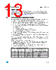
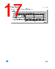
13 / 44 page  M95128, M95128-W, M95128-R Operating features 13/44 4.2 Status Register Figure 3 shows the position of the Status Register in the control logic of the device. The Status Register contains a number of status and control bits that can be read or set (as appropriate) by specific instructions. For a detailed description of the Status Register bits, see Section 5.3: Read Status Register (RDSR). 4.3 Data Protection and protocol control Non-volatile memory devices can be used in environments that are particularly noisy, and within applications that could experience problems if memory bytes are corrupted. Consequently, the device features the following data protection mechanisms: ● Write and Write Status Register instructions are checked that they consist of a number of clock pulses that is a multiple of eight, before they are accepted for execution. ● All instructions that modify data must be preceded by a Write Enable (WREN) instruction to set the Write Enable Latch (WEL) bit. This bit is returned to its reset state by the following events: –Power-up – Write Disable (WRDI) instruction completion – Write Status Register (WRSR) instruction completion – Write (WRITE) instruction completion ● The Block Protect (BP1, BP0) bits in the Status Register allow part of the memory to be configured as read-only. ● The Write Protect (W) signal is used to protect the Block Protect (BP1, BP0) bits of the Status Register. For any instruction to be accepted, and executed, Chip Select (S) must be driven High after the rising edge of Serial Clock (C) for the last bit of the instruction, and before the next rising edge of Serial Clock (C). Two points need to be noted in the previous sentence: ● The ‘last bit of the instruction’ can be the eighth bit of the instruction code, or the eighth bit of a data byte, depending on the instruction (except for Read Status Register (RDSR) and Read (READ) instructions). ● The ‘next rising edge of Serial Clock (C)’ might (or might not) be the next bus transaction for some other device on the SPI bus. Table 2. Write-protected block size Status Register bits Protected block Array addresses protected BP1 BP0 M95128, M95128-W, M95128-R 0 0 none none 0 1 Upper quarter 3000h - 3FFFh 1 0 Upper half 2000h - 3FFFh 1 1 Whole memory 0000h - 3FFFh |
|
链接网址 |
| ALLDATASHEET是否为您带来帮助? [ DONATE ] |
关于 Alldatasheet | 广告服务 | 联系我们 | 隐私政策 | 数据表链接 | 链接交换 | 制造商名单 All Rights Reserved©Alldatasheet.com |
| Russian : Alldatasheetru.com | Korean : Alldatasheet.co.kr | Spanish : Alldatasheet.es | French : Alldatasheet.fr | Italian : Alldatasheetit.com Portuguese : Alldatasheetpt.com | Polish : Alldatasheet.pl | Vietnamese : Alldatasheet.vn Indian : Alldatasheet.in | Mexican : Alldatasheet.com.mx | British : Alldatasheet.co.uk | New Zealand : Alldatasheet.co.nz |
|
Family Site : ic2ic.com |
icmetro.com |
 Chinese ▼
 English
 Chinese
 German
 Japanese
 Russian
 Korean
 Spanish
 French
 Italian
 Portuguese
 Polish
 Vietnamese
 Indian
 Mexican
 British
 New Zealand