|
数据搜索系统,热门电子元器件搜索 |
|
|
数据搜索系统,热门电子元器件搜索 |
|
BQ20Z95 数据表(PDF) 5 Page - Texas Instruments |
|
|
|
|||||||||||||||||||||||||||||
BQ20Z95 数据表(HTML) 5 Page - Texas Instruments |
|
|
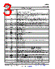
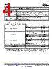
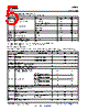
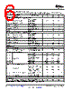
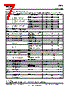
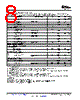
5 / 20 page  www.ti.com Recommended Operating Conditions Electrical Characteristics bq20z95 SLUS757 – JULY 2007 over operating free-air temperature range (unless otherwise noted) PARAMETER PIN MIN NOM MAX UNIT VSS Supply voltage VCC, VBAT 4.5 25 V V(STARTUP) Minimum startup voltage VCC, BAT, PACK 5.5 V VC(n)-VC(n+1); n = 1,2,3,4 0 5 V VC1, VC2, VC3, VC4 0 VSUP V VIN Input Voltage Range VC5 0 0.5 V ASRN, ASRP –0.5 0.5 V PACK, PMS 0 25 V V(GPOD) Output Voltage Range GPOD 0 25 V A(GPOD) Drain Current(1) GPOD 1 mA C(REG25) 2.5V LDO Capacitor REG25 1 µF C(REG33) 3.3V LDO Capacitor REG33 2.2 µF C(VCELL+) Cell Voltage Output Capacitor VCELL+ 0.1 µF C(PACK) PACK input block resistor(2) PACK 1 k Ω (1) Use an external resistor to limit the current to GPOD to 1mA in high voltage application. (2) Use an external resistor to limit the inrush current PACK pin required. over operating free-air temperature range (unless otherwise noted), TA = –40°C to 85°C, V(REG25) = 2.41 V to 2.59 V, V(BAT) = 14 V, C(REG25) = 1 µF, C(REG33) = 2.2 µF; typical values at TA = 25°C (unless otherwise noted) PARAMETER TEST CONDITIONS MIN TYP MAX UNIT SUPPLY CURRENT I(NORMAL) Firmware running 550 µA I(SLEEP) Sleep Mode CHG FET on; DSG FET on 124 µA CHG FET off; DSG FET on 90 µA CHG FET off; DSG FET off 52 µA I(SHUTDOWN) Shutdown Mode 0.1 1 µA SHUTDOWN WAKE; TA = 25°C (unless otherwise noted) I(PACK) Shutdown exit at VSTARTUP threshold 1 µA SRx WAKE FROM SLEEP; TA = 25°C (unless otherwise noted) Positive or negative wake threshold V(WAKE) with 1.00 mV, 2.25 mV, 4.5 mV and 9 1.25 10 mV mV programmable options V(WAKE) = 1 mV; -0.7 0.7 I(WAKE)= 0, RSNS1 = 0, RSNS0 = 1; V(WAKE) = 2.25 mV; I(WAKE) = 1, RSNS1 = 0, RSNS0 = 1; -0.8 0.8 I(WAKE) = 0, RSNS1 = 1, RSNS0 = 0; V(WAKE_ACR) Accuracy of V(WAKE) mV V(WAKE) = 4.5 mV; I(WAKE) = 1, RSNS1 = 1, RSNS0 = 1; -1.0 1.0 I(WAKE) = 0, RSNS1 = 1, RSNS0 = 0; V(WAKE) = 9 mV; -1.4 1.4 I(WAKE) = 1, RSNS1 = 1, RSNS0 = 1; V(WAKE_TCO) Temperature drift of V(WAKE) accuracy 0.5 %/ °C Time from application of current and t(WAKE) 1 10 ms wake of bq8040 POWER-ON RESET VIT– Negative-going voltage input Voltage at REG25 pin 1.70 1.80 1.90 V Vhys Hysteresis VIT+ – VIT- 50 150 250 mV active low time after power up or tRST RESET active low time 100 250 560 µs watchdog reset WATCHDOG TIMER tWDTINT Watchdog start up detect time 250 500 1000 ms Copyright © 2007, Texas Instruments Incorporated Submit Documentation Feedback 5 Product Folder Link(s): bq20z95 |
|
|
链接网址 |
| ALLDATASHEET是否为您带来帮助? [ DONATE ] |
关于 Alldatasheet | 广告服务 | 联系我们 | 隐私政策 | 数据表链接 | 链接交换 | 制造商名单 All Rights Reserved©Alldatasheet.com |
| Russian : Alldatasheetru.com | Korean : Alldatasheet.co.kr | Spanish : Alldatasheet.es | French : Alldatasheet.fr | Italian : Alldatasheetit.com Portuguese : Alldatasheetpt.com | Polish : Alldatasheet.pl | Vietnamese : Alldatasheet.vn Indian : Alldatasheet.in | Mexican : Alldatasheet.com.mx | British : Alldatasheet.co.uk | New Zealand : Alldatasheet.co.nz |
|
Family Site : ic2ic.com |
icmetro.com |
 Chinese ▼
 English
 Chinese
 German
 Japanese
 Russian
 Korean
 Spanish
 French
 Italian
 Portuguese
 Polish
 Vietnamese
 Indian
 Mexican
 British
 New Zealand