|
数据搜索系统,热门电子元器件搜索 |
|
|
数据搜索系统,热门电子元器件搜索 |
|
STDRIVEG611 数据表(PDF) 13 Page - STMicroelectronics |
|
|
|||||||||||||||||||||||||||||
STDRIVEG611 数据表(HTML) 13 Page - STMicroelectronics |
|
|
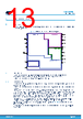
13 / 33 page  6 Device description 6.1 Device structure Figure 10 is a simplified version of the block diagram of STDRIVEG611. It consists of basic structures described in the following sections. Figure 10. STDRIVEG611 simplified block diagram UVLO VCC Logic, interlocking UVLO VCCL Driver Level Shifter VCCL Regulator Driver Level Shifter GND VCC HIN LIN BOOT RONH OUTH OUT VCCH RONL OUTL PGND FLT OverTemperature Protection STBY VCCL Regulator VCCL CIN + REF V + - Comparator filter smartSD SSD SD UVLO-READY OVERTEMP SD/OD OD UVLO VCCH VCCH Regulator LOGIC SECTION HIGH SIDE DRIVER LOW SIDE DRIVER COMPARATOR &SMARTSD 6.1.1 Logic section This section receives the input signals, manages the system protections (UVLOs, comparator and overtemperature), and transfers the input pulses to relevant drivers through level shifters. It is electrically referred to the GND pin and supplied by the VCC pin. 6.1.2 Low-side driver This block receives input pulses from the logic section through the level shifter and provides driving action to the low-side GaN transistor. It is electrically referred to PGND, that must be connected to the source (preferably Kelvin) of the low-side GaN transistor. GaN VGS sink current can be tuned with the RGATE resistor placed between the OUTL and GaN gate. Source current can be tuned with the RON resistor between VCCL and RONL. Sink path impedance is the sum of RGATE and driver RSI, while source path impedance is the total of RON, RGATE, and driver RSO. Tuning RON is typically done to adjust hard turn-on dV/dt. Tuning RGATE is typically done to eventually dump VGS ringing at turn-off, to adjust hard turn-off dV/dt while avoiding induced turn-on at high-side hard turn-on. Low-side driver circuitry is supplied by VCC, while an integrated voltage regulator tightly stabilizes the supply voltage of the output stage of the driver (VLS). A UVLO comparator interrupts the half-bridge activity if the regulator’s output voltage is insufficient for a proper GaN’s driving. See Section 6.4.2 for a detailed LS UVLO protection description. The low-side driver has been designed to allow the use of current sense resistors without affecting the applied VGS voltage. STDRIVEG611 Device description DS14457 - Rev 2 page 13/33 |
|
链接网址 |
| ALLDATASHEET是否为您带来帮助? [ DONATE ] |
关于 Alldatasheet | 广告服务 | 联系我们 | 隐私政策 | 数据表链接 | 链接交换 | 制造商名单 All Rights Reserved©Alldatasheet.com |
| Russian : Alldatasheetru.com | Korean : Alldatasheet.co.kr | Spanish : Alldatasheet.es | French : Alldatasheet.fr | Italian : Alldatasheetit.com Portuguese : Alldatasheetpt.com | Polish : Alldatasheet.pl | Vietnamese : Alldatasheet.vn Indian : Alldatasheet.in | Mexican : Alldatasheet.com.mx | British : Alldatasheet.co.uk | New Zealand : Alldatasheet.co.nz |
|
Family Site : ic2ic.com |
icmetro.com |
 Chinese ▼
 English
 Chinese
 German
 Japanese
 Russian
 Korean
 Spanish
 French
 Italian
 Portuguese
 Polish
 Vietnamese
 Indian
 Mexican
 British
 New Zealand