|
数据搜索系统,热门电子元器件搜索 |
|
|
数据搜索系统,热门电子元器件搜索 |
|
STM32F412RGY3TR 数据表(PDF) 88 Page - STMicroelectronics |
|
|
|||||||||||||||||||||||||||||
STM32F412RGY3TR 数据表(HTML) 88 Page - STMicroelectronics |
|
|
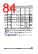
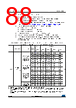
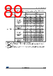
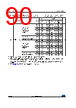
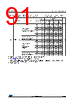
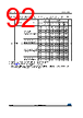
88 / 201 page  Electrical characteristics STM32F412xE/G 88/201 DocID028087 Rev 7 Typical and maximum current consumption The MCU is placed under the following conditions: • All I/O pins are in input mode with a static value at VDD or VSS (no load). • All peripherals are disabled except if it is explicitly mentioned. • The Flash memory access time is adjusted to both fHCLK frequency and VDD ranges (refer to Table 17: Features depending on the operating power supply range). • The voltage scaling is adjusted to fHCLK frequency as follows: – Scale 3 for fHCLK ≤ 64 MHz – Scale 2 for 64 MHz < fHCLK ≤ 84 MHz – Scale 1 for 84 MHz < fHCLK ≤ 100 MHz • The system clock is HCLK, fPCLK1 = fHCLK/2, and fPCLK2 = fHCLK. • External clock is 4 MHz and PLL is ON except if it is explicitly mentioned. • The maximum values are obtained for VDD = 3.6 V and a maximum ambient temperature (TA), and the typical values for TA= 25 °C and VDD = 3.3 V unless otherwise specified. Table 22. Typical and maximum current consumption, code with data processing (ART accelerator disabled) running from SRAM - VDD = 1.7 V Symbol Parameter Conditions fHCLK (MHz) Typ Max(1) Unit TA= 25 °C TA= 25 °C TA= 85 °C TA= 105 °C TA= 125 °C IDD Supply current in Run mode External clock, PLL ON, all peripherals enabled(2)(3) 100 28.1 30.24 31.27 32.21 34.21 mA 84 22.7 24.05 24.54 25.11 26.74 64 15.7 16.99 17.47 18.03 19.71 50 12.3 13.36 13.82 14.36 15.51 25 6.5 7.44 7.82 8.30 8.96 20 5.6 6.16 6.66 7.20 7.77 HSI, PLL off, all peripherals enabled(2)(3) 16 3.9 4.70 5.31 6.08 6.57 1 0.6 0.78 1.33 1.98 2.14 External clock, PLL ON, all peripherals disabled(3) 100 14.0 15.48 16.08 16.83 18.51 84 11.3 12.23 12.75 13.41 16.09 64 7.9 8.84 9.31 10.01 11.61 50 6.2 7.06 7.53 8.19 9.50 25 3.4 4.18 4.61 5.13 5.95 20 2.9 3.44 3.98 4.65 5.39 HSI, PLL off, all peripherals disabled(3) 16 2.0 2.51 3.13 3.89 4.51 1 0.5 0.64 1.21 1.90 2.21 1. Based on characterization, not tested in production unless otherwise specified 2. When analog peripheral blocks such as ADC, HSE, LSE, HSI, or LSI are ON, an additional power consumption has to be considered. 3. When the ADC is ON (ADON bit set in the ADC_CR2 register), add an additional power consumption of 1.6 mA for the analog part. |
|
链接网址 |
| ALLDATASHEET是否为您带来帮助? [ DONATE ] |
关于 Alldatasheet | 广告服务 | 联系我们 | 隐私政策 | 数据表链接 | 链接交换 | 制造商名单 All Rights Reserved©Alldatasheet.com |
| Russian : Alldatasheetru.com | Korean : Alldatasheet.co.kr | Spanish : Alldatasheet.es | French : Alldatasheet.fr | Italian : Alldatasheetit.com Portuguese : Alldatasheetpt.com | Polish : Alldatasheet.pl | Vietnamese : Alldatasheet.vn Indian : Alldatasheet.in | Mexican : Alldatasheet.com.mx | British : Alldatasheet.co.uk | New Zealand : Alldatasheet.co.nz |
|
Family Site : ic2ic.com |
icmetro.com |
 Chinese ▼
 English
 Chinese
 German
 Japanese
 Russian
 Korean
 Spanish
 French
 Italian
 Portuguese
 Polish
 Vietnamese
 Indian
 Mexican
 British
 New Zealand