|
数据搜索系统,热门电子元器件搜索 |
|
|
数据搜索系统,热门电子元器件搜索 |
|
STM32F429NET6 数据表(PDF) 28 Page - STMicroelectronics |
|
|
|||||||||||||||||||||||||||||
STM32F429NET6 数据表(HTML) 28 Page - STMicroelectronics |
|
|
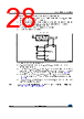
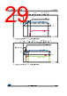
28 / 231 page  Functional overview STM32F427xx STM32F429xx 28/231 DocID024030 Rev 6 In regulator OFF mode, the following features are no more supported: • PA0 cannot be used as a GPIO pin since it allows to reset a part of the V12 logic power domain which is not reset by the NRST pin. • As long as PA0 is kept low, the debug mode cannot be used under power-on reset. As a consequence, PA0 and NRST pins must be managed separately if the debug connection under reset or pre-reset is required. • The over-drive and under-drive modes are not available. • The Standby mode is not available. Figure 8. Regulator OFF The following conditions must be respected: • VDD should always be higher than VCAP_1 and VCAP_2 to avoid current injection between power domains. • If the time for VCAP_1 and VCAP_2 to reach V12 minimum value is faster than the time for VDD to reach 1.7 V, then PA0 should be kept low to cover both conditions: until VCAP_1 and VCAP_2 reach V12 minimum value and until VDD reaches 1.7 V (see Figure 9). • Otherwise, if the time for VCAP_1 and VCAP_2 to reach V12 minimum value is slower than the time for VDD to reach 1.7 V, then PA0 could be asserted low externally (see Figure 10). • If VCAP_1 and VCAP_2 go below V12 minimum value and VDD is higher than 1.7 V, then a reset must be asserted on PA0 pin. Note: The minimum value of V12 depends on the maximum frequency targeted in the application (see Table 17: General operating conditions). |
|
链接网址 |
| ALLDATASHEET是否为您带来帮助? [ DONATE ] |
关于 Alldatasheet | 广告服务 | 联系我们 | 隐私政策 | 数据表链接 | 链接交换 | 制造商名单 All Rights Reserved©Alldatasheet.com |
| Russian : Alldatasheetru.com | Korean : Alldatasheet.co.kr | Spanish : Alldatasheet.es | French : Alldatasheet.fr | Italian : Alldatasheetit.com Portuguese : Alldatasheetpt.com | Polish : Alldatasheet.pl | Vietnamese : Alldatasheet.vn Indian : Alldatasheet.in | Mexican : Alldatasheet.com.mx | British : Alldatasheet.co.uk | New Zealand : Alldatasheet.co.nz |
|
Family Site : ic2ic.com |
icmetro.com |
 Chinese ▼
 English
 Chinese
 German
 Japanese
 Russian
 Korean
 Spanish
 French
 Italian
 Portuguese
 Polish
 Vietnamese
 Indian
 Mexican
 British
 New Zealand