IP113M LF
Preliminary Data Sheet
30/58
April 9, 2007
Copyright © 2004, IC Plus Corp.
IP113M LF-DS-R11
3.1
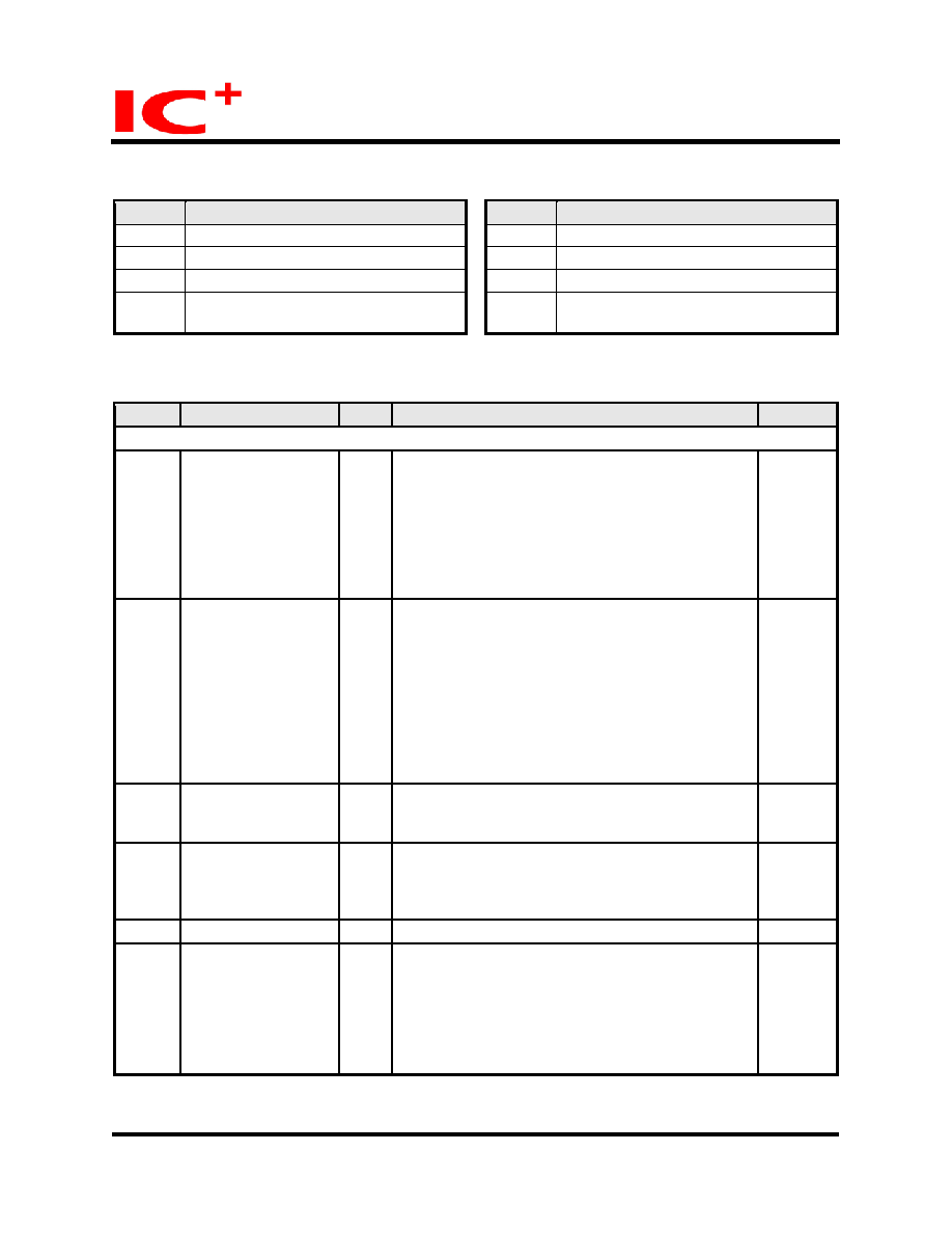
The basic MII registers
Type
Description
Type
Description
R/W
Read/Write
RC
Read and Clear
SC
Self-Clearing
LL
Latching Low
RO
Read Only
LH
Latching High
Pin(1)
The default value is “1” and it depends
on the setting of its corresponding pin.
Pin(0)
The default value is “0” and it depends
on the setting of its corresponding pin.
The basic MII registers 0
MII
NAME
R/W
DESCRIPTION
DEFAULT
MII control register (address 00h)
0.15
Reset
R/W
SC
1 = PHY reset
0 = normal operation
This bit is self-clearing, IP113M LF will return a
value of 1 before reset process is completed, and
will not accept any write transaction of MII
Management within reset process. Make any
change to Auto-Negotiation or speed mode will
cause IP113M LF reset again.
0
0.14
Loop back
R/W
1 = Loop back mode
0 = normal operation
When this bit is set, IP113M LF will be isolated
from the network media, and the assertion of
TXEN at the MII will not transmit data on the
network. All MII transmit data path will return to MII
receive data path in response to the assertion of
TXEN. MII COL signal will remain de-asserted at
all times, unless bit 0.7 (Collision Test) is set. Use
has to wait about 100ms for loop back path ready.
0
0.13
Speed Selection
RW
1 = 100Mbps
0 = 10Mbps
It is valid only if bit 0.12 is set to be 0.
Pin(1)
0.12
Auto-Negotiation
Enable
RW
1 = Auto-Negotiation Enable
0 = Auto-Negotiation Disable
MII register 16.11 auto-MDI/MDIX should be
disabled if auto-negotiation is disabled.
1
0.11
Reserved
R/W
This bit should be “0” for normal operation.
0
0.10
Isolate
R/W
1 = electrically isolate PHY from MII
0 = normal operation
When this bit is setting to 1, IP113M LF will be
isolated from MII, and not respond to the TXD[3:0]
and
TXEN and keep CRS, RXDV and RXD[3:0]
in
high
impedance,
but
will
respond
to
management transactions.
0

 Chinese ▼
 English
 Chinese
 German
 Japanese
 Russian
 Korean
 Spanish
 French
 Italian
 Portuguese
 Polish
 Vietnamese
 Indian
 Mexican
 British
 New Zealand


