|
数据搜索系统,热门电子元器件搜索 |
|
|
数据搜索系统,热门电子元器件搜索 |
|
LM4865M/NOPB.A 数据表(PDF) 4 Page - Texas Instruments |
|
|
|||||||||||||||||||||||||||||
LM4865M/NOPB.A 数据表(HTML) 4 Page - Texas Instruments |
|
|
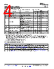
4 / 30 page  LM4865 SNAS035G – DECEMBER 1999 – REVISED MAY 2013 www.ti.com ELECTRICAL CHARACTERISTICS (1) (2) The following specifications apply for VDD = 5V, unless otherwise specified. Limits apply for TA = 25°C. LM4865 Symbol Parameter Conditions Min(3) Typical(4) Max(3) Units VDD Supply Voltage 2.7 5.5 V VIN = 0V, IO = 0A, HP Sense = 0V 4 7 mA IDD Quiescent Power Supply Current VIN = 0V, IO - 0A, HP Sense = 5V 3.5 6 mA ISD Shutdown Current VPIN4 ≤ 0.3V 0.7 µA VOS Output Offset Voltage VIN = 0V 5 50 mV THD = 1% (max), HP Sense < 0.8V, f = 500 750 mW 1kHz, RL = 8Ω THD = 10% (max), HP Sense < 0.8V, f = 1.0 W 1kHz, RL = 8Ω PO Output Power THD + N = 1%, HP Sense > 4V, 80 mW f = 1kHz, RL = 32Ω THD = 10%, HP Sense > 4V, 110 mW f = 1kHz, RL = 32Ω PO = 300 mWrms, f = 20Hz–20kHz, RL = THD+N Total Harmonic Distortion + Noise 0.6 % 8 Ω VRIPPLE = 200mVrms, RL = 8Ω, CB = 1.0 PSRR Power Supply Rejection Ratio 50 dB µF, f = 1kHz Gain with VPIN4 ≥ 4.0V, (80% of VDD) 18.8 20 dB GainRANGE Single-Ended Gain Range Gain with VPIN4 ≤ 0.9V, (18% of VDD) −70 −72 dB VIH HP Sense High Input Voltage 4 V VIL HP Sense Low Input Voltage 0.8 V (1) All voltages are measured with respect to the ground pin, unless otherwise specified. (2) Absolute Maximum Ratings indicate limits beyond which damage to the device may occur. Operating Ratings indicate conditions for which the device is functional, but do not ensure specific performance limits. Electrical Characteristics state DC and AC electrical specifications under particular test conditions that ensure specific performance limits. This assumes that the device operates within the Operating Ratings. Specifications are not ensured for parameters where no limit is given. The typical value, however, is a good indication of device performance. (3) Limits are ensured to AOQL (Average Outgoing Quality Level). (4) Typicals are measured at 25°C and represent the parametric norm. EXTERNAL COMPONENTS DESCRIPTION (Figure 3 ) Components Functional Description 1. Ci Input coupling capacitor which blocks the DC voltage at the amplifier's input terminals. It also creates a highpass filter with the internal Ri. The designer should note that10kOhm<(Ri)<110kOhm.Therefore fc = 1/(2πRiCi). Refer to the section, PROPERLY SELECTING EXTERNAL COMPONENTS , for an explanation of how to determine the value of Ci. 2. CS Supply bypass capacitor which provides power supply filtering. Refer to the POWER SUPPLY BYPASSING section for information concerning proper placement and selection of the supply bypass capacitor. 3. CB Bypass pin capacitor which provides half-supply filtering. Refer to the section, PROPERLY SELECTING EXTERNAL COMPONENTS, for information concerning proper placement and selection of CB. 4 Submit Documentation Feedback Copyright © 1999–2013, Texas Instruments Incorporated Product Folder Links: LM4865 |
|
|
链接网址 |
| ALLDATASHEET是否为您带来帮助? [ DONATE ] |
关于 Alldatasheet | 广告服务 | 联系我们 | 隐私政策 | 数据表链接 | 链接交换 | 制造商名单 All Rights Reserved©Alldatasheet.com |
| Russian : Alldatasheetru.com | Korean : Alldatasheet.co.kr | Spanish : Alldatasheet.es | French : Alldatasheet.fr | Italian : Alldatasheetit.com Portuguese : Alldatasheetpt.com | Polish : Alldatasheet.pl | Vietnamese : Alldatasheet.vn Indian : Alldatasheet.in | Mexican : Alldatasheet.com.mx | British : Alldatasheet.co.uk | New Zealand : Alldatasheet.co.nz |
|
Family Site : ic2ic.com |
icmetro.com |
 Chinese ▼
 English
 Chinese
 German
 Japanese
 Russian
 Korean
 Spanish
 French
 Italian
 Portuguese
 Polish
 Vietnamese
 Indian
 Mexican
 British
 New Zealand