|
数据搜索系统,热门电子元器件搜索 |
|
|
数据搜索系统,热门电子元器件搜索 |
|
SN74LVC74APWRE4 数据表(PDF) 10 Page - Texas Instruments |
|
|
|||||||||||||||||||||||||||||
SN74LVC74APWRE4 数据表(HTML) 10 Page - Texas Instruments |
|
|
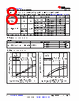
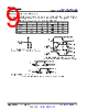
10 / 46 page  7 Detailed Description 7.1 Overview The SNx4LVC74A devices feature two independent positive-edge triggered D flip-flops. Integrated preset ( PRE) and clear ( CLR) functions allow for easy setup and control during operation. The SN54LVC74A device is specified from –55°C to 125°C, and the SN74LVC74A device is specified from –40°C to 125°C. A low level at the preset ( PRE) or clear ( CLR) inputs sets or resets the outputs, regardless of the levels of the other inputs. When PRE and CLR are inactive (high), data at the data (D) input meeting the setup time requirements is transferred to the outputs on the positive-going edge of the clock pulse. Clock triggering occurs at a voltage level and is not directly related to the rise time of the clock pulse. Following the hold-time interval, data at the D input can be changed without affecting the levels at the outputs. The data I/Os and control inputs are overvoltage tolerant. This feature allows the use of these devices for down-translation in a mixed-voltage environment. 7.2 Functional Block Diagram Copyright © 2016, Texas Instruments Incorporated 7.3 Feature Description A low level at the preset ( PRE) or clear ( CLR) inputs sets or resets the outputs, regardless of the levels of the other inputs. When PRE and CLR are inactive (high), data at the data (D) input meeting the setup time requirements is transferred to the outputs on the positive-going edge of the clock pulse. Clock triggering occurs at a voltage level and is not directly related to the rise time of the clock pulse. Following the hold-time interval, data at the D input can be changed without affecting the levels at the outputs. 7.4 Device Functional Modes Table 7-1 describes the SNx4LVC74A functionality and interactions between the PRE, CLR, CLK, and D inputs. Table 7-1. Function Table INPUTS OUTPUTS PRE CLR CLK D Q Q L H X X H L H L X X L H L L X X H(1) H(1) H H ↑ H H L SN54LVC74A, SN74LVC74A SCAS287W – JANUARY 1993 – REVISED DECEMBER 2024 www.ti.com 10 Submit Document Feedback Copyright © 2024 Texas Instruments Incorporated Product Folder Links: SN54LVC74A SN74LVC74A |
|
链接网址 |
| ALLDATASHEET是否为您带来帮助? [ DONATE ] |
关于 Alldatasheet | 广告服务 | 联系我们 | 隐私政策 | 数据表链接 | 链接交换 | 制造商名单 All Rights Reserved©Alldatasheet.com |
| Russian : Alldatasheetru.com | Korean : Alldatasheet.co.kr | Spanish : Alldatasheet.es | French : Alldatasheet.fr | Italian : Alldatasheetit.com Portuguese : Alldatasheetpt.com | Polish : Alldatasheet.pl | Vietnamese : Alldatasheet.vn Indian : Alldatasheet.in | Mexican : Alldatasheet.com.mx | British : Alldatasheet.co.uk | New Zealand : Alldatasheet.co.nz |
|
Family Site : ic2ic.com |
icmetro.com |
 Chinese ▼
 English
 Chinese
 German
 Japanese
 Russian
 Korean
 Spanish
 French
 Italian
 Portuguese
 Polish
 Vietnamese
 Indian
 Mexican
 British
 New Zealand