|
数据搜索系统,热门电子元器件搜索 |
|
|
数据搜索系统,热门电子元器件搜索 |
|
GS-R51515S 数据表(PDF) 5 Page - STMicroelectronics |
|
|
|||||||||||||||||||||||||||||
GS-R51515S 数据表(HTML) 5 Page - STMicroelectronics |
|
|
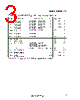
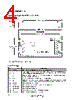
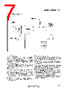
5 / 8 page  5/8 USER NOTES Input Voltage The recommended operating maximum DC input voltage is 40V inclusive of the ripple voltage. The use of an external low ESR, high ripple current capacitor located as close the module as possible is recommended; suggested value is 100 µF/50V. Soft-start To avoid heavy inrush current the output voltage rise time is typically 10ms in any condition of load. Power Fail-Reset Circuit The module include a voltage sensing circuit that may be used to generate a power-on/power-off reset signal for a microprocessor system. The circuit sense the input supply voltage and the output generated voltage Vo1 (+5V) and will gener- ate the required reset signal only when both the sensed voltages have reached the required value for correct system operation. When both the supply voltage and the regulated voltage are in the correct range the output Reset signal is generated after a delay time tDR of 100ms typical. A latch assures that if a spike is present on the sensed voltage the delay time circuit discharges completely before initialization of a new reset cycle. Reset output has internal pull-up resistor of 10kOhm connected to Vo +5V pin. Maximum sink ou tput current is 20mA at VRESET(sat) = 200mV. Fig. 1 and fig. 2 show reset waveforms. Power Fail Programmable Input This pin is internally connected via a divider to the +Vin pin for Power Fail function. The factory setting is for a value of 11V with 1V hysteresis. It is possible to program a different value of Power Fail threshold by connecting a resistor (Rpf) be- tween pin 3 (Power Fail Input) and pin 1 (GND Input). The value of Rpf must be calculated accord- ing to the following formula: Rpf = 5.1 =(kΩ) Vpf − 5.1 34 − 0.191 where Vpf is the desired value of Power Fail thresh- old voltage. Exampe: Vpf = 24V (must not be lower than 12V): Rpf = 5.1 = 14kΩ 24 − 5.1 34 − 0.191 Figure 1 - Reset and Power Fail waveforms. GS-R51212S/GS-R51515S |
|
|
链接网址 |
| ALLDATASHEET是否为您带来帮助? [ DONATE ] |
关于 Alldatasheet | 广告服务 | 联系我们 | 隐私政策 | 数据表链接 | 链接交换 | 制造商名单 All Rights Reserved©Alldatasheet.com |
| Russian : Alldatasheetru.com | Korean : Alldatasheet.co.kr | Spanish : Alldatasheet.es | French : Alldatasheet.fr | Italian : Alldatasheetit.com Portuguese : Alldatasheetpt.com | Polish : Alldatasheet.pl | Vietnamese : Alldatasheet.vn Indian : Alldatasheet.in | Mexican : Alldatasheet.com.mx | British : Alldatasheet.co.uk | New Zealand : Alldatasheet.co.nz |
|
Family Site : ic2ic.com |
icmetro.com |
 Chinese ▼
 English
 Chinese
 German
 Japanese
 Russian
 Korean
 Spanish
 French
 Italian
 Portuguese
 Polish
 Vietnamese
 Indian
 Mexican
 British
 New Zealand