|
数据搜索系统,热门电子元器件搜索 |
|
|
数据搜索系统,热门电子元器件搜索 |
|
AD8027ART-R2 数据表(PDF) 19 Page - Analog Devices |
|
|
|||||||||||||||||||||||||||||
AD8027ART-R2 数据表(HTML) 19 Page - Analog Devices |
|
|
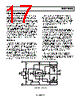
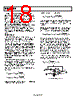
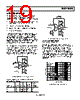
19 / 24 page  AD8027/AD8028 Rev. C | Page 19 of 24 WIDEBAND OPERATION Voltage feedback amplifiers can use a wide range of resistor values to set their gain. Proper design of the application’s feedback network requires consideration of the following issues: • Poles formed by the amplifier’s input capacitances with the resistances seen at the amplifier’s input terminals • Effects of mismatched source impedances • Resistor value impact on the application’s voltage noise • Amplifier loading effects The AD8027/AD8028 have an input capacitance of 2 pF. This input capacitance forms a pole with the amplifier’s feedback network, destabilizing the loop. For this reason, it is generally desirable to keep the source resistances below 500 Ω, unless some capacitance is included in the feedback network. Likewise, keeping the source resistances low also takes advantage of the AD8027/AD8028’s low input referred voltage noise of 4.3 nV/√Hz. With a wide bandwidth of over 190 MHz, the AD8027/AD8028 have numerous applications and configurations. The AD8027/ AD8028 part shown in Figure 57 is configured as a noninvert- ing amplifier. An easy selection table of gain, resistor values, bandwidth, slew rate, and noise performance is presented in Table 5, and the inverting configuration is shown in Figure 58. +V –V C2 10 μF C1 0.1 μF C4 0.1 μF C3 10 μF VOUT RG R1 RF SELECT VIN R1 = RF||RG AD8027/ AD8028 + – 03327-A-056 Figure 57. Wideband Noninverting Gain Configuration Table 5. Component Values, Bandwidth, and Noise Performance (VS = ±2.5 V) Noise Gain (Noninverting) RSOURCE (Ω) RF (Ω) RG (Ω) –3 dB SS BW (MHz) Output Noise with Resistors (nV/√Hz) 1 50 0 N/A 190 4.4 2 50 499 499 95 10 10 50 499 54.9 13 45 +V –V C2 10 μF C1 0.1 μF C4 0.1 μF C3 10 μF R1 C5 VOUT RG R1 = RF||RG RF VIN SELECT AD8027/ AD8028 + – 03327-A-057 CF Figure 58. Wideband Inverting Gain Configuration CIRCUIT CONSIDERATIONS Balanced Input Impedances Balanced input impedances can help to improve distortion performance. When the amplifier transitions from PNP pair to NPN pair operation, a change in both the magnitude and direction of the input bias current occurs. When multiplied times imbalanced input impedances, a change in offset can result. The key to minimizing this distortion is to keep the input impedances balanced on both inputs. Figure 59 shows the effect of the imbalance and degradation in distortion performance for a 50 Ω source impedance, with and without a 50 Ω balanced feedback path. FREQUENCY (MHz) 0.1 1 10 20 –100 –90 –80 –70 –60 –50 –40 –30 –20 G = +1 VOUT = 2V p-p RL = 1kΩ VS = +3V RF = 24.9Ω RF = 49.9Ω RF = 0Ω 03327-A-058 Figure 59. SFDR vs. Frequency and Various RF |
|
|
链接网址 |
| ALLDATASHEET是否为您带来帮助? [ DONATE ] |
关于 Alldatasheet | 广告服务 | 联系我们 | 隐私政策 | 数据表链接 | 链接交换 | 制造商名单 All Rights Reserved©Alldatasheet.com |
| Russian : Alldatasheetru.com | Korean : Alldatasheet.co.kr | Spanish : Alldatasheet.es | French : Alldatasheet.fr | Italian : Alldatasheetit.com Portuguese : Alldatasheetpt.com | Polish : Alldatasheet.pl | Vietnamese : Alldatasheet.vn Indian : Alldatasheet.in | Mexican : Alldatasheet.com.mx | British : Alldatasheet.co.uk | New Zealand : Alldatasheet.co.nz |
|
Family Site : ic2ic.com |
icmetro.com |
 Chinese ▼
 English
 Chinese
 German
 Japanese
 Russian
 Korean
 Spanish
 French
 Italian
 Portuguese
 Polish
 Vietnamese
 Indian
 Mexican
 British
 New Zealand