|
数据搜索系统,热门电子元器件搜索 |
|
|
数据搜索系统,热门电子元器件搜索 |
|
AD8031ARTZ-R2 数据表(PDF) 13 Page - Analog Devices |
|
|
|||||||||||||||||||||||||||||
AD8031ARTZ-R2 数据表(HTML) 13 Page - Analog Devices |
|
|
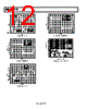
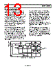
13 / 20 page  AD8031/AD8032 Rev. C | Page 13 of 20 THEORY OF OPERATION The AD8031/AD8032 are single and dual versions of high speed, low power, voltage feedback amplifiers featuring an innovative architecture that maximizes the dynamic range capability on the inputs and outputs. The linear input common- mode range exceeds either supply voltage by 200 mV, and the amplifiers show no phase reversal up to 500 mV beyond supply. The output swings to within 20 mV of either supply when driving a light load; 300 mV when driving up to 5 mA. Switching to the NPN pair as the common-mode voltage is driven beyond 1 V within the positive supply allows the amplifier to provide useful operation for signals at either end of the supply voltage range and eliminates the possibility of phase reversal for input signals up to 500 mV beyond either power supply. Offset voltage also changes to reflect the offset of the input pair in control. The transition region is small, approximately 180 mV. These sudden changes in the dc parameters of the input stage can produce glitches that adversely affect distortion. Fabricated on Analog Devices, Inc. eXtra Fast Complementary Bipolar (XFCB) process, the amplifier provides an impressive 80 Hz bandwidth when used as a follower and a 30 V/μs slew rate at only 800 μA supply current. Careful design allows the amplifier to operate with a supply voltage as low as 2.7 V. OVERDRIVING THE INPUT STAGE Sustained input differential voltages greater than 3.4 V should be avoided as the input transistors can be damaged. Input clamp diodes are recommended if the possibility of this condition exists. INPUT STAGE OPERATION A simplified schematic of the input stage appears in Figure 43. For common-mode voltages up to 1.1 V within the positive supply (0 V to 3.9 V on a single 5 V supply), tail current I2 flows through the PNP differential pair, Q13 and Q17. Q5 is cut off; no bias current is routed to the parallel NPN differential pair, Q2 and Q3. As the common-mode voltage is driven within 1.1 V of the positive supply, Q5 turns on and routes the tail current away from the PNP pair and to the NPN pair. During this transition region, the input current of the amplifier changes magnitude and direction. Reusing the same tail current ensures that the input stage has the same transconductance, which determines the gain and bandwidth of the amplifier, in both regions of operation. The voltages at the collectors of the input pairs are set to 200 mV from the power supply rails. This allows the amplifier to remain in linear operation for input voltages up to 500 mV beyond the supply voltages. Driving the input common-mode voltage beyond that point will forward bias the collector junction of the input transistor, resulting in phase reversal. Sustaining this condition for any length of time should be avoided because it is easy to exceed the maximum allowed input differential voltage when the amplifier is in phase reversal. Q3 Q2 Q13 Q17 Q6 Q8 Q10 4 Q14 4 1 1 Q7 Q15 1 Q11 4 1 4 Q16 Q18 Q4 VCC VIN VIP Q5 Q9 VEE OUTPUT STAGE, COMMON-MODE FEEDBACK R4 2kΩ R2 2kΩ R1 2kΩ I3 25µA I4 25µA R3 2kΩ I1 5µA I2 90µA 1.1V R5 50kΩ R6 850Ω R7 850Ω R8 850Ω R9 850Ω Figure 43. Simplified Schematic of AD8031 Input Stage |
|
|
链接网址 |
| ALLDATASHEET是否为您带来帮助? [ DONATE ] |
关于 Alldatasheet | 广告服务 | 联系我们 | 隐私政策 | 数据表链接 | 链接交换 | 制造商名单 All Rights Reserved©Alldatasheet.com |
| Russian : Alldatasheetru.com | Korean : Alldatasheet.co.kr | Spanish : Alldatasheet.es | French : Alldatasheet.fr | Italian : Alldatasheetit.com Portuguese : Alldatasheetpt.com | Polish : Alldatasheet.pl | Vietnamese : Alldatasheet.vn Indian : Alldatasheet.in | Mexican : Alldatasheet.com.mx | British : Alldatasheet.co.uk | New Zealand : Alldatasheet.co.nz |
|
Family Site : ic2ic.com |
icmetro.com |
 Chinese ▼
 English
 Chinese
 German
 Japanese
 Russian
 Korean
 Spanish
 French
 Italian
 Portuguese
 Polish
 Vietnamese
 Indian
 Mexican
 British
 New Zealand