|
数据搜索系统,热门电子元器件搜索 |
|
|
数据搜索系统,热门电子元器件搜索 |
|
AD8515ARTZ-R2 数据表(PDF) 14 Page - Analog Devices |
|
|
|||||||||||||||||||||||||||||
AD8515ARTZ-R2 数据表(HTML) 14 Page - Analog Devices |
|
|
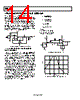
14 / 16 page  AD8515 Rev. D | Page 14 of 16 A MICROPOWER REFERENCE VOLTAGE GENERATOR Many single-supply circuits are configured with the circuit biased to one-half of the supply voltage. In these cases, a false ground reference can be created by using a voltage divider buffered by an amplifier. Figure 35 shows the schematic for such a circuit. The two 1 MΩ resistors generate the reference voltages while drawing only 0.9 μA of current from a 1.8 V supply. A capacitor connected from the inverting terminal to the output of the op amp provides compensation to allow for a bypass capacitor to be connected at the reference output. This bypass capacitor helps establish an ac ground for the reference output. AD8515 C3 1µF C2 0.022µF C1 1µF R3 10kΩ R2 1MΩ R4 100Ω 1.8V TO 5V 0.9V TO 2.5V R1 1MΩ 3 4 1 U1 V+ V– + – Figure 35. Micropower Voltage Reference Generator A 100 kHz SINGLE-SUPPLY SECOND-ORDER BAND-PASS FILTER The circuit in Figure 36 is commonly used in portable applica- tions where low power consumption and wide bandwidth are required. This figure shows a circuit for a single-supply band-pass filter with a center frequency of 100 kHz. It is essential that the op amp have a loop gain at 100 kHz to maintain an accurate center frequency. This loop gain requirement necessitates the choice of an op amp with a high unity gain crossover frequency, such as the AD8515. The 4.5 MHz bandwidth of the AD8515 is sufficient to accurately produce the 100 kHz center frequency, as the response in Figure 37 shows. When the op amp bandwidth is close to the center frequency of the filter, the amplifier internal phase shift causes excess phase shift at 100 kHz, altering the filter response. In fact, if the chosen op amp has a bandwidth close to 100 kHz, the phase shift of the op amps causes the loop to oscillate. A common-mode bias level is easily created by connecting the noninverting input to a resistor divider consisting of two resistors connected between VCC and ground. This bias point is also decoupled to ground with a 1 μF capacitor. C1 R1 f L × × π = 2 1 C1 R1 f H × × π = 2 1 R2 R1 H + = 1 0 V 5 V 8 . 1 − = VCC where: fL is the low −3 dB frequency. fH is the high −3 dB frequency. H0 is the midfrequency gain. 400mV V11 VCC VCC VOUT 0 0 R6 1MΩ R8 1MΩ C3 1µF C1 2nF R1 5kΩ R2 20kΩ R5 2kΩ AD8515 3 4 1 U9 V+ V– + – C6 10pF Figure 36. Second-Order Band-Pass Filter 2 0 1k 10k 100M FREQUENCY (Hz) 100k 1M 10M 1.5 1 0.5 Figure 37. Frequency Response of the Band-Pass Filter |
|
|
链接网址 |
| ALLDATASHEET是否为您带来帮助? [ DONATE ] |
关于 Alldatasheet | 广告服务 | 联系我们 | 隐私政策 | 数据表链接 | 链接交换 | 制造商名单 All Rights Reserved©Alldatasheet.com |
| Russian : Alldatasheetru.com | Korean : Alldatasheet.co.kr | Spanish : Alldatasheet.es | French : Alldatasheet.fr | Italian : Alldatasheetit.com Portuguese : Alldatasheetpt.com | Polish : Alldatasheet.pl | Vietnamese : Alldatasheet.vn Indian : Alldatasheet.in | Mexican : Alldatasheet.com.mx | British : Alldatasheet.co.uk | New Zealand : Alldatasheet.co.nz |
|
Family Site : ic2ic.com |
icmetro.com |
 Chinese ▼
 English
 Chinese
 German
 Japanese
 Russian
 Korean
 Spanish
 French
 Italian
 Portuguese
 Polish
 Vietnamese
 Indian
 Mexican
 British
 New Zealand