|
数据搜索系统,热门电子元器件搜索 |
|
|
数据搜索系统,热门电子元器件搜索 |
|
AD8091ART-R2 数据表(PDF) 13 Page - Analog Devices |
|
|
|||||||||||||||||||||||||||||
AD8091ART-R2 数据表(HTML) 13 Page - Analog Devices |
|
|
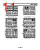
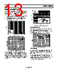
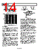
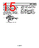
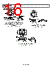
13 / 20 page  AD8091/AD8092 Rev. C | Page 13 of 20 DRIVING CAPACITIVE LOADS A highly capacitive load reacts with the output of the amplifiers, causing a loss in phase margin and subsequent peaking or even oscillation, as shown in Figure 29 and Figure 30. There are two methods to effectively minimize its effect. • Put a small value resistor in series with the output to isolate the load capacitor from the amplifier’s output stage. • Increase the phase margin with higher noise gains or by adding a pole with a parallel resistor and capacitor from −IN to the output. 8 –12 –10 –8 –6 –4 –2 0 2 4 6 0.1 500 100 110 FREQUENCY (MHz) VS = 5V G = +1 RL = 2kΩ CL = 50pF VO = 200mV p-p Figure 29. Closed-Loop Frequency Response: CL = 50 pF 2.50V 100ns 50mV 2.60V 2.45V 2.55V 2.40V VS = 5V G = +1 RL = 2kΩ CL = 50pF Figure 30. 200 mV Step Response: CL = 50 pF As the closed-loop gain is increased, the larger phase margin allows for large capacitor loads with less peaking. Adding a low value resistor in series with the load at lower gains has the same effect. Figure 31 shows the effect of a series resistor for various voltage gains. For large capacitive loads, the frequency response of the amplifier is dominated by the series resistor and capaci- tive load. 10000 1 10 100 1000 16 5 23 4 ACL (V/V) VS = 5V £30% OVERSHOOT RS = 3Ω RS = 0Ω RG RF RS CL VOUT 50Ω VIN 100mV STEP Figure 31. Capacitive Load Drive vs. Closed-Loop Gain OVERDRIVE RECOVERY Overdrive of an amplifier occurs when the output range and/or input range is exceeded. The amplifier must recover from this overdrive condition. The AD8091/AD8092 recover within 60 ns from negative overdrive and within 45 ns from positive overdrive, as shown in Figure 32. V/DIV AS SHOWN 100ns INPUT 1V/DIV OUTPUT 2V/DIV VS = ±5V G = +5 RF = 2kΩ RL = 2kΩ Figure 32. Overdrive Recovery ACTIVE FILTERS Active filters at higher frequencies require wider bandwidth op amps to work effectively. Excessive phase shift produced by lower frequency op amps can significantly impact active filter performance. Figure 33 shows an example of a 2 MHz biquad bandwidth filter that uses three op amps. Such circuits are sometimes used in medical ultrasound systems to lower the noise bandwidth of the analog signal before A/D conversion. Note that the unused amplifiers’ inputs should be tied to ground. |
|
|
链接网址 |
| ALLDATASHEET是否为您带来帮助? [ DONATE ] |
关于 Alldatasheet | 广告服务 | 联系我们 | 隐私政策 | 数据表链接 | 链接交换 | 制造商名单 All Rights Reserved©Alldatasheet.com |
| Russian : Alldatasheetru.com | Korean : Alldatasheet.co.kr | Spanish : Alldatasheet.es | French : Alldatasheet.fr | Italian : Alldatasheetit.com Portuguese : Alldatasheetpt.com | Polish : Alldatasheet.pl | Vietnamese : Alldatasheet.vn Indian : Alldatasheet.in | Mexican : Alldatasheet.com.mx | British : Alldatasheet.co.uk | New Zealand : Alldatasheet.co.nz |
|
Family Site : ic2ic.com |
icmetro.com |
 Chinese ▼
 English
 Chinese
 German
 Japanese
 Russian
 Korean
 Spanish
 French
 Italian
 Portuguese
 Polish
 Vietnamese
 Indian
 Mexican
 British
 New Zealand