|
数据搜索系统,热门电子元器件搜索 |
|
|
数据搜索系统,热门电子元器件搜索 |
|
UPC277G2 数据表(PDF) 3 Page - Renesas Technology Corp |
|
|
|||||||||||||||||||||||||||||
UPC277G2 数据表(HTML) 3 Page - Renesas Technology Corp |
|
|
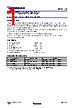
3 / 9 page  UPC277G2, UPC393G2 R03DS0132EJ0200 Rev.2.00 Page 3 of 8 Feb.4.25 RECOMMENDED OPERATING CONDITIONS Parameter Symbol MIN. TYP. MAX. Unit Power Supply Voltage (Dual Supply) V ± ±1 ±16 V Power Supply Voltage (V - = GND) V + +2 +32 V ELECTRICAL CHARACTERISTICS UPC277G2, UPC393G2 (TA = 25 °C, V + = +5 V, V - = GND) Parameter Symbol MIN. TYP. MAX. Unit Test Condition Input Offset Voltage VIO ±2 ±5 mV VO = 1.4 V, VREF = 1.4 V, RS = 0 Ω Input Offset Current IIO ±5 ±50 nA VO ≒ 1.4 V Input Bias Current Note 6 IB 25 250 nA VO ≒ 1.4 V Large Signal Voltage Gain AV 200000 RL = 15 kΩ Circuit Current Note 7 ICC 0.6 1 mA RL = ∞, IO = 0 A Common Mode Input Voltage Range VICM 0 V + -1.5 V Output Saturation Voltage VOL 0.2 0.4 V VI(-) = +1 V, VI(+) = 0 V, IO SINK = 4 mA Output Sink Current IO SINK 6 16 mA VI(-) = +1 V, VI(+) = 0 V, VO ≤ 1.5 V Output Leakage Current IO LEAK 0.1 nA VI(+) = +1 V, VI(-) = 0 V, VO = 5 V Pulse Response Time Note 8 1.3 μs RL = 5.1 kΩ, VRL = 5 V UPC277G2(5), UPC393G2(5) (TA = 25 °C, V + = +5 V, V - = GND) Parameter Symbol MIN. TYP. MAX. Unit Test Condition Input Offset Voltage VIO ±2 ±2.5 mV VO = 1.4 V, VREF = 1.4 V, RS = 0 Ω Input Offset Current IIO ±5 ±50 nA VO ≒ 1.4 V Input Bias Current Note 6 IB 25 60 nA VO ≒ 1.4 V Large Signal Voltage Gain AV 200000 RL = 15 kΩ Circuit Current Note 7 ICC 0.6 0.8 mA RL = ∞, IO = 0 A Common Mode Input Voltage Range VICM 0 V + -1.4 V Output Saturation Voltage VOL1 0.2 V VI(-) = +1 V, VI(+) = 0 V, IO SINK = 4 mA VOL2 1.5 V VI(-) = +1 V, VI(+) = 0 V, IO SINK = 10 mA Output Sink Current IO SINK 10 16 mA VI(-) = +1 V, VI(+) = 0 V, VO ≤ 1.5 V Output Leakage Current IO LEAK 0.1 100 nA VI(+) = +1 V, VI(-) = 0 V, VO = 5 V Response Time Note 8 1.3 μs RL = 5.1 kΩ, VRL = 5 V 【 Note】 6. The current flow direction of the input bias is out from the IC because the first stage of the IC composed of PNP transistor. The current value is the value when the differential amplified circuit of the input stage is balanced. When the comparator is active, twice the amount of current will flow to the pin with lower potential. 7. Current flowing through the internal circuit. This current flow regardless of the channel used. 8. Values when the input amplitude is 100 mV and the overdrive is 5 mV. Increasing the overdrive can shorten the response time. |
|
|
链接网址 |
| ALLDATASHEET是否为您带来帮助? [ DONATE ] |
关于 Alldatasheet | 广告服务 | 联系我们 | 隐私政策 | 数据表链接 | 链接交换 | 制造商名单 All Rights Reserved©Alldatasheet.com |
| Russian : Alldatasheetru.com | Korean : Alldatasheet.co.kr | Spanish : Alldatasheet.es | French : Alldatasheet.fr | Italian : Alldatasheetit.com Portuguese : Alldatasheetpt.com | Polish : Alldatasheet.pl | Vietnamese : Alldatasheet.vn Indian : Alldatasheet.in | Mexican : Alldatasheet.com.mx | British : Alldatasheet.co.uk | New Zealand : Alldatasheet.co.nz |
|
Family Site : ic2ic.com |
icmetro.com |
 Chinese ▼
 English
 Chinese
 German
 Japanese
 Russian
 Korean
 Spanish
 French
 Italian
 Portuguese
 Polish
 Vietnamese
 Indian
 Mexican
 British
 New Zealand