|
数据搜索系统,热门电子元器件搜索 |
|
|
数据搜索系统,热门电子元器件搜索 |
|
UPC277G25-AP 数据表(PDF) 7 Page - Renesas Technology Corp |
|
|
|||||||||||||||||||||||||||||
UPC277G25-AP 数据表(HTML) 7 Page - Renesas Technology Corp |
|
|
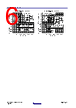
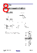
7 / 9 page  UPC277G2, UPC393G2 R03DS0132EJ0200 Rev.2.00 Page 7 of 8 Feb.4.25 USE WITH PRECAUTIONS • Managing unused circuits If there is an unused circuit, the following connection is recommended. Process example of unused circuits • Ratings of input/output pin voltage When the voltage of input/output pin exceeds the absolute maximum rating, the parasitic diode within the IC may conduct, causing characteristics degradation or damage. In addition, if the input pin is lower than V−, or the output pin exceeds the power supply voltage, it is recommended to make a clamping circuit using a diode with low forward voltage (e.g.: Schottky diode) as protection. • Range of common-mode input voltage When the supply voltage does not meet the condition of electrical characteristics, the range of common-mode input voltage is as follows. VICM (TYP.): V - ~ V + -1.5 [V] (TA = 25 °C) During designing, do include some tolerance by considering temperature characteristics etc. • Range of input current The “Input Bias Current [IB]” specified in the electric characteristic table, is the average current value flowing to the +input pin [IN] and the - input pin [II] when the operation amplifier input stage are balanced (in a state where negative feedback is applied). When the comparator is active, the input stage of the differential amplified circuit will not be balance during comparison, the amount of input current flow is twice the amount to the pin with lower potential. • Handling of ICs When stress is added to the ICs due to warpage or bending of a board, the characteristic may fluctuates due to piezoelectric effect. Therefore, pay attention to warpage or bending of a board. OUT (オープン) V - - + 同相入力電圧範囲 (VICM) 内の電位へ V - V + (open) To potentials within the range of common-mode input voltage (VICM) |
|
|
链接网址 |
| ALLDATASHEET是否为您带来帮助? [ DONATE ] |
关于 Alldatasheet | 广告服务 | 联系我们 | 隐私政策 | 数据表链接 | 链接交换 | 制造商名单 All Rights Reserved©Alldatasheet.com |
| Russian : Alldatasheetru.com | Korean : Alldatasheet.co.kr | Spanish : Alldatasheet.es | French : Alldatasheet.fr | Italian : Alldatasheetit.com Portuguese : Alldatasheetpt.com | Polish : Alldatasheet.pl | Vietnamese : Alldatasheet.vn Indian : Alldatasheet.in | Mexican : Alldatasheet.com.mx | British : Alldatasheet.co.uk | New Zealand : Alldatasheet.co.nz |
|
Family Site : ic2ic.com |
icmetro.com |
 Chinese ▼
 English
 Chinese
 German
 Japanese
 Russian
 Korean
 Spanish
 French
 Italian
 Portuguese
 Polish
 Vietnamese
 Indian
 Mexican
 British
 New Zealand