|
数据搜索系统,热门电子元器件搜索 |
|
|
数据搜索系统,热门电子元器件搜索 |
|
AD8639ARMZ-R2 数据表(PDF) 14 Page - Analog Devices |
|
|
|||||||||||||||||||||||||||||
AD8639ARMZ-R2 数据表(HTML) 14 Page - Analog Devices |
|
|
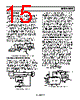
14 / 20 page  AD8638/AD8639 Rev. C | Page 14 of 20 THEORY OF OPERATION The AD8638/AD8639 are single-supply and dual-supply, ultrahigh precision, rail-to-rail output operational amplifiers. The typical offset voltage of 3 μV allows the amplifiers to be easily configured for high gains without risk of excessive output voltage errors. The extremely small temperature drift of 30 nV/°C ensures a minimum offset voltage error over the entire temperature range of −40°C to +125°C, making the amplifiers ideal for a variety of sensitive measurement applications in harsh operating environments. The AD8638/AD8639 achieve a high degree of precision through a patented auto-zeroing topology. This unique topology allows the AD8638/AD8639 to maintain low offset voltage over a wide temperature range and over the operating lifetime. The AD8638/AD8639 also optimize the noise and bandwidth over previous generations of auto-zero amplifiers, offering the lowest voltage noise of any auto-zero amplifier by more than 50%. Previous designs used either auto-zeroing or chopping to add precision to the specifications of an amplifier. Auto-zeroing results in low noise energy at the auto-zeroing frequency, at the expense of higher low frequency noise due to aliasing of wide- band noise into the auto-zeroed frequency band. Chopping results in lower low frequency noise at the expense of larger noise energy at the chopping frequency. The AD8638/AD8639 use both auto-zeroing and chopping in a patented ping-pong arrangement to obtain lower low frequency noise together with lower energy at the chopping and auto-zeroing frequencies, maximizing the SNR for the majority of applications without the need for additional filtering. The relatively high clock frequency of 15 kHz simplifies filter requirements for a wide, useful, noise-free bandwidth. The AD8638 is among the few auto-zero amplifiers offered in the 5-lead SOT-23 package. This provides significant improve- ment over the ac parameters of previous auto-zero amplifiers. The AD8638/AD8639 have low noise over a relatively wide bandwidth (0 Hz to 10 kHz) and can be used where the highest dc precision is required. In systems with signal bandwidths ranging from 5 kHz to 10 kHz, the AD8638/AD8639 provide true 16-bit accuracy, making this device the best choice for very high resolution systems. 1/f NOISE 1/f noise, also known as pink noise, is a major contributor to errors in dc-coupled measurements. This 1/f noise error term can be in the range of several microvolts or more and, when amplified by the closed-loop gain of the circuit, can show up as a large output signal. For example, when an amplifier with 5 μV p-p 1/f noise is configured for a gain of 1000, its output has 5 mV of error due to the 1/f noise. However, the AD8638/AD8639 eliminate 1/f noise internally and thus significantly reduce output errors. The internal elimination of 1/f noise is accomplished as follows: 1/f noise appears as a slowly varying offset to AD8638/AD8639 inputs. Auto-zeroing corrects any dc or low frequency offset. Therefore, the 1/f noise component is essentially removed, leaving the AD8638/AD8639 free of 1/f noise. INPUT VOLTAGE RANGE The AD8638/AD8639 are not rail-to-rail input amplifiers; therefore, care is required to ensure that both inputs do not exceed the input voltage range. Under normal negative feedback operating conditions, the amplifier corrects its output to ensure that the two inputs are at the same voltage. However, if either input exceeds the input voltage range, the loop opens and large currents begin to flow through the ESD protection diodes in the amplifier. These diodes are connected between the inputs and each supply rail to protect the input transistors against an electrostatic discharge event, and they are normally reverse-biased. However, if the input voltage exceeds the supply voltage, these ESD diodes can become forward-biased. Without current limiting, excessive amounts of current may flow through these diodes, causing permanent damage to the device. If inputs are subject to over- voltage, insert appropriate series resistors to limit the diode current to less than 5 mA maximum. OUTPUT PHASE REVERSAL Output phase reversal occurs in some amplifiers when the input common-mode voltage range is exceeded. As common-mode voltage is moved outside the common-mode range, the outputs of these amplifiers can suddenly jump in the opposite direction to the supply rail. This is the result of the differential input pair shutting down, causing a radical shifting of internal voltages that results in the erratic output behavior. The AD8638/AD8639 amplifiers have been carefully designed to prevent any output phase reversal if both inputs are main- tained within the specified input voltage range. If one or both inputs exceed the input voltage range but remain within the supply rails, an internal loop opens and the output varies. Therefore, the inputs should always be less than at least 2 V below the positive supply. OVERLOAD RECOVERY TIME Many auto-zero amplifiers are plagued by a long overload recovery time, often in milliseconds, due to the complicated settling behavior of the internal nulling loops after saturation of the outputs. The AD8638/AD8639 are designed so that internal settling occurs within two clock cycles after output saturation happens. This results in a much shorter recovery time, less than 50 μs, when compared to other auto-zero amplifiers. The wide bandwidth of the AD8638/AD8639 enhances performance when the parts are used to drive loads that inject transients into the outputs. This is a common situation when an amplifier is used to drive the input of switched capacitor ADCs. |
|
|
链接网址 |
| ALLDATASHEET是否为您带来帮助? [ DONATE ] |
关于 Alldatasheet | 广告服务 | 联系我们 | 隐私政策 | 数据表链接 | 链接交换 | 制造商名单 All Rights Reserved©Alldatasheet.com |
| Russian : Alldatasheetru.com | Korean : Alldatasheet.co.kr | Spanish : Alldatasheet.es | French : Alldatasheet.fr | Italian : Alldatasheetit.com Portuguese : Alldatasheetpt.com | Polish : Alldatasheet.pl | Vietnamese : Alldatasheet.vn Indian : Alldatasheet.in | Mexican : Alldatasheet.com.mx | British : Alldatasheet.co.uk | New Zealand : Alldatasheet.co.nz |
|
Family Site : ic2ic.com |
icmetro.com |
 Chinese ▼
 English
 Chinese
 German
 Japanese
 Russian
 Korean
 Spanish
 French
 Italian
 Portuguese
 Polish
 Vietnamese
 Indian
 Mexican
 British
 New Zealand