|
数据搜索系统,热门电子元器件搜索 |
|
|
数据搜索系统,热门电子元器件搜索 |
|
STPCATLAS 数据表(PDF) 102 Page - STMicroelectronics |
|
|
|||||||||||||||||||||||||||||
STPCATLAS 数据表(HTML) 102 Page - STMicroelectronics |
|
|
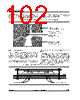
102 / 111 page  DESIGN GUIDELINES 102/111 Issue 1.0 - July 24, 2002 To avoid solder wicking over to the via pads during soldering, it is important to have a solder mask of 4 mil around the pad (NSMD pad). This gives a diameter of 33 mil for a 25 mil ground pad. To obtain the optimum ground layout, place the vias directly under the ball pads. In this case no local board distortion is tolerated. 6.4.5.3. Heat dissipation The thickness of the copper on PCB layers is typically 34 µm for external layers and 17 µm for internal layers. This means that thermal dissipation is not good; high board temperatures are concentrated around the devices and these fall quickly with increased distance. Where possible, place a metal layer inside the PCB; this improves dramatically the spread of heat and hence the thermal dissipation of the board. The possibility of using the whole system box for thermal dissipation is very useful in cases of high internal temperatures and low outside temperatures. Bottom side of the PBGA should be thermally connected to the metal chassis in order to propagate the heat flow through the metal. Thermally connecting also the top side will improve furthermore the heat dissipation. Figure 6-35 illustrates such an implementation. Figure 6-34. Optimum Layout for Central Ground Ball - top layer Via to Ground layer Pad for ground ball Clearance = 6mil diameter = 25 mil hole diameter = 14 mil Solder mask diameter = 33 mil External diameter = 37 mil connections = 10 mil Figure 6-35. Use of Metal Plate for Thermal Dissipation Metal planes Thermal conductor Board Die |
|
链接网址 |
| ALLDATASHEET是否为您带来帮助? [ DONATE ] |
关于 Alldatasheet | 广告服务 | 联系我们 | 隐私政策 | 数据表链接 | 链接交换 | 制造商名单 All Rights Reserved©Alldatasheet.com |
| Russian : Alldatasheetru.com | Korean : Alldatasheet.co.kr | Spanish : Alldatasheet.es | French : Alldatasheet.fr | Italian : Alldatasheetit.com Portuguese : Alldatasheetpt.com | Polish : Alldatasheet.pl | Vietnamese : Alldatasheet.vn Indian : Alldatasheet.in | Mexican : Alldatasheet.com.mx | British : Alldatasheet.co.uk | New Zealand : Alldatasheet.co.nz |
|
Family Site : ic2ic.com |
icmetro.com |
 Chinese ▼
 English
 Chinese
 German
 Japanese
 Russian
 Korean
 Spanish
 French
 Italian
 Portuguese
 Polish
 Vietnamese
 Indian
 Mexican
 British
 New Zealand