|
数据搜索系统,热门电子元器件搜索 |
|
|
数据搜索系统,热门电子元器件搜索 |
|
AT28BV256-20PI 数据表(PDF) 5 Page - ATMEL Corporation |
|
|
|||||||||||||||||||||||||||||
AT28BV256-20PI 数据表(HTML) 5 Page - ATMEL Corporation |
|
|
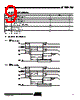
5 / 18 page  5 0273J–PEEPR–10/06 AT28BV256 5.6.1 Hardware Protection Hardware features protect against inadvertent writes to the AT28BV256 in the following ways: (a) V CC power-on delay – once VCC has reached 1.8V (typical) the device will automatically time out 10 ms (typical) before allowing a write; (b) write inhibit – holding any one of OE low, CE high or WE high inhibits write cycles; and (c) noise filter – pulses of less than 15 ns (typical) on the WE or CE inputs will not initiate a write cycle. 5.6.2 Software Data Protection A software-controlled data protection feature has been implemented on the AT28BV256. Soft- ware data protection (SDP) helps prevent inadvertent writes from corrupting the data in the device. SDP can prevent inadvertent writes during power-up and power-down as well as any other potential periods of system instability. The AT28BV256 can only be written using the software data protection feature. A series of three write commands to specific addresses with specific data must be presented to the device before writing in the byte or page mode. The same three write commands must begin each write opera- tion. All software write commands must obey the page mode write timing specifications. The data in the 3-byte command sequence is not written to the device; the address in the command sequence can be utilized just like any other location in the device. Any attempt to write to the device without the 3-byte sequence will start the internal write timers. No data will be written to the device; however, for the duration of t WC, read operations will effec- tively be polling operations. 5.7 Device Identification An extra 64 bytes of EEPROM memory are available to the user for device identification. By rais- ing A9 to 12V ± 0.5V and using address locations 7FC0H to 7FFFH the additional bytes may be written to or read from in the same manner as the regular memory array. |
|
|
链接网址 |
| ALLDATASHEET是否为您带来帮助? [ DONATE ] |
关于 Alldatasheet | 广告服务 | 联系我们 | 隐私政策 | 数据表链接 | 链接交换 | 制造商名单 All Rights Reserved©Alldatasheet.com |
| Russian : Alldatasheetru.com | Korean : Alldatasheet.co.kr | Spanish : Alldatasheet.es | French : Alldatasheet.fr | Italian : Alldatasheetit.com Portuguese : Alldatasheetpt.com | Polish : Alldatasheet.pl | Vietnamese : Alldatasheet.vn Indian : Alldatasheet.in | Mexican : Alldatasheet.com.mx | British : Alldatasheet.co.uk | New Zealand : Alldatasheet.co.nz |
|
Family Site : ic2ic.com |
icmetro.com |
 Chinese ▼
 English
 Chinese
 German
 Japanese
 Russian
 Korean
 Spanish
 French
 Italian
 Portuguese
 Polish
 Vietnamese
 Indian
 Mexican
 British
 New Zealand