|
数据搜索系统,热门电子元器件搜索 |
|
|
数据搜索系统,热门电子元器件搜索 |
|
ASM3I622S00AG-08-SR 数据表(PDF) 1 Page - PulseCore Semiconductor |
|
|
|||||||||||||||||||||||||||||
ASM3I622S00AG-08-SR 数据表(HTML) 1 Page - PulseCore Semiconductor |
|
|
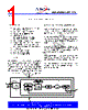
1 / 16 page  May 2007 ASM3P622S00A/B/J/E/K rev 0.4 Notice: The information in this document is subject to change without notice. PulseCore Semiconductor Corporation 1715 S. Bascom Ave Suite 200 Campbell, CA 95008 • Tel: 408-879-9077 • Fax: 408-879-9018 www.pulsecoresemi.com Low Frequency Timing-Safe™ Peak EMI reduction IC General Features • Low Frequency Clock distribution with Timing- Safe™ Peak EMI Reduction • Input frequency range: 4MHz - 20MHz • Zero input - output propagation delay • Low-skew outputs • Output-output skew less than 250pS • Device-device skew less than 700pS • Less than 200pS cycle-to-cycle jitter • Available in 16pin, 150mil SOIC, 4.4mm TSSOP (ASM3P622S00E/K), and in 8pin, 150 mil SOIC, 4.4mm TSSOP Packages (ASM3P622S00A/B/J) • 3.3V Operation • Industrial temperature range • Advanced CMOS technology • The First True Drop-in Solution Functional Description ASM3P622S00A/B/J/E/K is a versatile, 3.3V Zero-delay buffer designed to distribute low frequency Timing-Safe™ clocks with Peak EMI reduction. ASM3P622S00E/K accepts one reference input and drives out eight low-skew clocks. It is available in a 16pin Package. The ASM3P622S00A/B/J is the eight-pin version and accepts one reference input and drives out one low-skew clock. All parts have on-chip PLLs that lock to an input clock on the XIN/CLKIN pin. The PLL feedback is on-chip and is obtained from the CLKOUT pad, internal to the device. Multiple ASM3P622S00E/K devices can accept the same input clock and distribute it. In this case, the skew between the outputs of the two devices is guaranteed to be less than 700pS. All outputs have less than 200pS of Cycle-to-cycle jitter. The input and output propagation delay is guaranteed to be less than ±350pS, and the output-to-output skew is guaranteed to be less than 250pS. Refer “Spread Spectrum Control and Input-Output Skew Table” for deviations and Input-Output Skew for ASM3P622S00A/B/J and ASM3P622S00E/K devices The ASM3P622S00A/B/J and ASM3P622S00E/K are available in two different packages, as shown in the ordering information table. Block Diagram GND Reference Divider Feedback Divider Modulation Phase Detector Loop Filter VCO Feedforward Divider PLL VDD CLKOUT SSON SS% XIN/CLKIN Crystal Oscillator XOUT |
类似零件编号 - ASM3I622S00AG-08-SR |
|
类似说明 - ASM3I622S00AG-08-SR |
|
|
|
链接网址 |
| ALLDATASHEET是否为您带来帮助? [ DONATE ] |
关于 Alldatasheet | 广告服务 | 联系我们 | 隐私政策 | 数据表链接 | 链接交换 | 制造商名单 All Rights Reserved©Alldatasheet.com |
| Russian : Alldatasheetru.com | Korean : Alldatasheet.co.kr | Spanish : Alldatasheet.es | French : Alldatasheet.fr | Italian : Alldatasheetit.com Portuguese : Alldatasheetpt.com | Polish : Alldatasheet.pl | Vietnamese : Alldatasheet.vn Indian : Alldatasheet.in | Mexican : Alldatasheet.com.mx | British : Alldatasheet.co.uk | New Zealand : Alldatasheet.co.nz |
|
Family Site : ic2ic.com |
icmetro.com |
 Chinese ▼
 English
 Chinese
 German
 Japanese
 Russian
 Korean
 Spanish
 French
 Italian
 Portuguese
 Polish
 Vietnamese
 Indian
 Mexican
 British
 New Zealand